S2S 2: Fabrication
Last Updated: 2025-07-01
Introduction
How do we take basic elements, purified to their elemental form, and imbue them with intelligence? How do we construct these magical slabs of electronic logic that power our modern world?
The answer strains the imagination. Modern SM is dazzlingly complex from any perspective. Leading node chips live at the very outermost boundary of what is physically possible. Thousands of steps, hundreds of billions in investment dollars, atomic precision, immense power, and tight multinational coordination. Fabrication of modern ICs is a (perhaps unparalleled) marvel of human engineering.
This piece will cover the following to give an in depth understanding of IC fabrication:
- Step by step explanation of how current cutting edge ICs are manufactured
- A summary quantification of the industry for context
- Detailed specifics on some of the most important companies in the space (TSMC, ASML)
- Current limitations and design frontiers
- Geopolitical bottlenecks & US dominance
Context
The fundamental challenge of SM since its inception has been the construction of machines that allow for useful computation. In the early days, "useful computation" comprised mainframes the size of a small home, vacuum tube transistors, and magnetic tape memory. The size, cost, and limited capabilities of these early computers heavily constrained the domain of their usefulness to very specific military and academic applications. Since that point, all advances in SM can be seen to be in service of expanding that domain by making ICs (and by extension computers) more capable, more economical, and more compact.
This has been done primarily by reducing the size of the fundamental components of modern computers, namely transistors and the logical circuits they are used to form, to successively smaller and smaller sizes. We have done so with remarkable consistency for the last 6 decades. It is this shrinking that Moore's law describes. And it's this shrinking that is principally responsible for the exponentially expanding useful domain of computation. While in the early days of SM we were able to increase transistor count with simple optimizations, we are now approaching the fundamental limitations of the universe. The dimensions of vacuum tube transistors could be measured in inches. Modern FinFET transistors are measured in atoms. Achieving this level of precision has required hundreds of billions of dollars in R&D and capital expenditure. We've had to reinvent every step in the process multiple times over.
It is a worthwhile aside to observe that very few processes, physical goods, or phenomena contain the capacity for this degree of improvement or optimization. Internal combustion engines cannot be made to be a million times more efficient or compact. Farming cannot reasonably be done with 1/1000th the land we currently use. Semiconductors are unique in this regard - not only was it possible to make ICs from the 50s and 60s billions of times better, we can also do so economically and with seemingly inexhaustible demand. This is a truly unique property, and points to something quite fundamental about the nature of computation, intelligence, and the universe.
What is a chip?
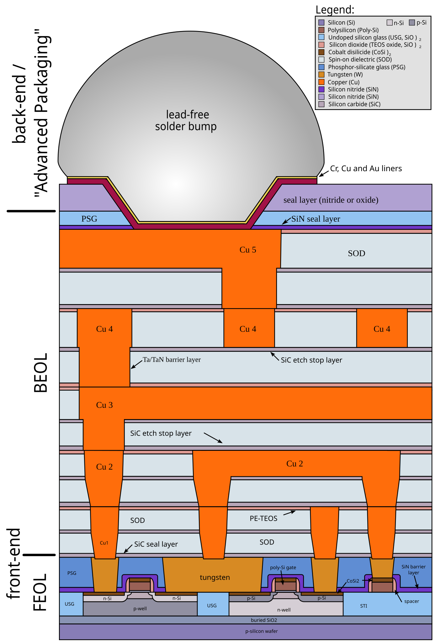
A useful analogy for modern semiconductors is a tiny, multilayered cake. The base layer is transistors, the essential logical building block of any computation. Arrayed above those transistors is a maze of snaking copper wires that connect the transistors into gates (think AND, OR, NOT, etc) and then connect those gates into larger circuits (think of bitwise addition or 64 bit multiplication modules). Generally speaking, each successive layer is more abstract in purpose than the preceding, and the final layers link together the largest, most general building blocks of the chip.
How are they built?
So, how do we construct these numerous layers? Each one is unique, and requires exacting precision, weaving different materials into each other. The answer is just that - layer by layer. SM process steps can be broken into a couple overarching categories:
- Material modification
- Material addition
- Masking
- Material removal
- Cleaning
- Inspecting
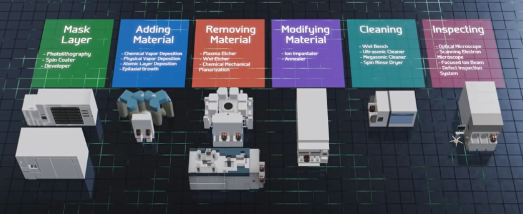
Save for masking, each of these 5 processes should be straightforward and obvious in their conceptual purpose. Each layer of the chip represents a cycle of these steps. In the following sections, I'll dive into each category and break down the machines and processes used for the leading edge node, and the companies that are involved. One broader categorization of these process steps is by grouping them chronologically based on when they are used in the chip production line, namely into steps that are Front-End of Line (FEOL), Back-End of Line (BEOL), or Middle of Line. FEOL steps are those that occur once at the beginning of the chip production line (initial wafer inspection and planing, transistor placement via ion doping). BEOL steps are similar, in that they are typically the final steps only applied once per chip (cutting out the chip dies from the wafer, packaging individual dies in their recognizable black plastic protective coating, final functional testing and binning). Middle of Line is where the bulk of the complexity lives, and is constituted by thousands or repeated steps to build the numerous interconnect layers.
Central Challenges
There are a handful of shared, central challenges that inform design decisions across almost every process step. Namely:
- Contamination causes defects, which in turn drive down yield
- Precision, consistency, and reliability are necessities
- Scale demands high levels of process parallelization
As a result, many different process steps (and their corresponding machines) share some common characteristics.
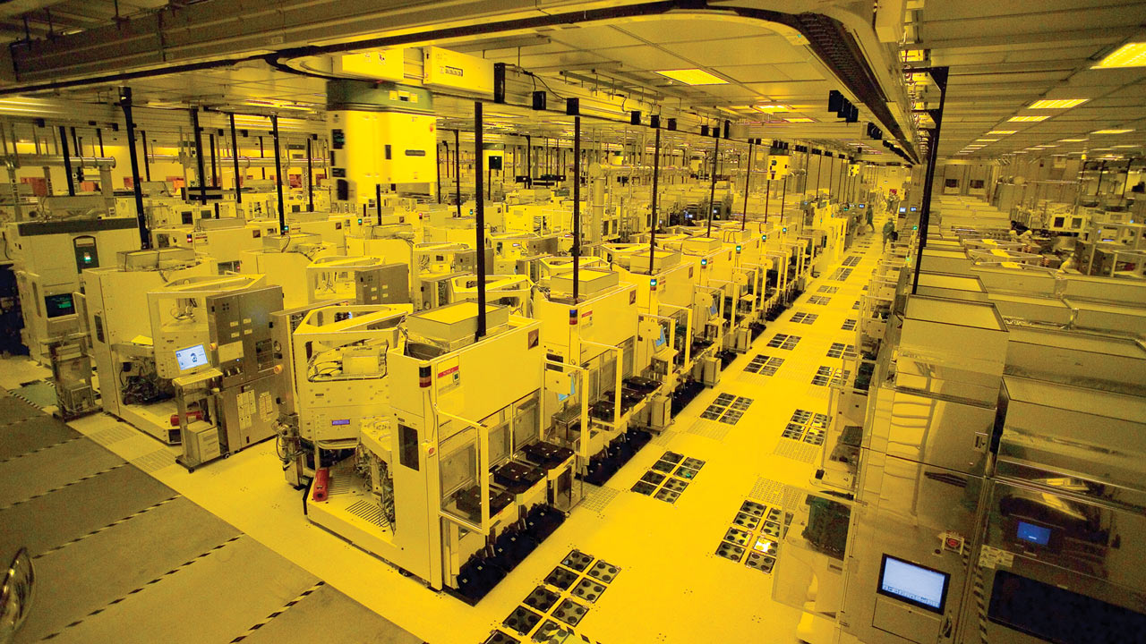
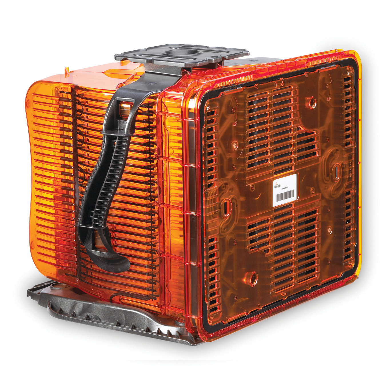
First, most process steps are performed under a vacuum and within the confines of a larger clean room. Between process steps, wafers are shuttled around foundries in hermetically sealed containers called front opening unified pods (FOUP) on a roof mounted rail system so as to make as little contact with the external environment as possible.
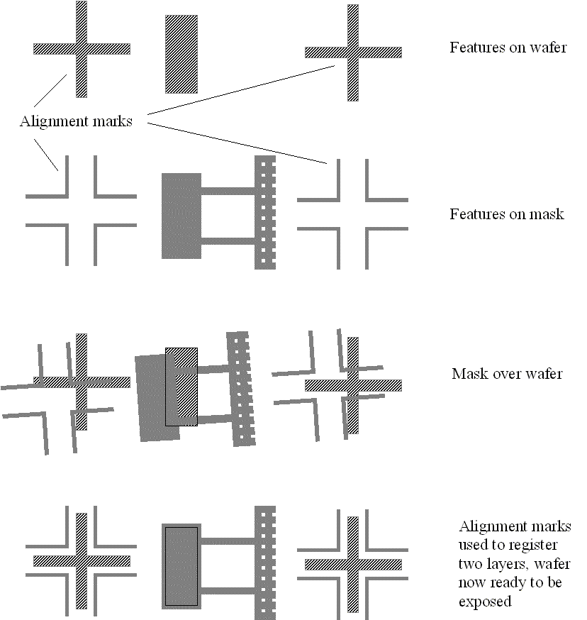
Second, process step actions must be extremely precise, consistent, and reliable. Machines at many process steps (especially litho) need to be tightly calibrated and capable of minute adjustments in the inevitable case of any misalignment. This means sensitivity levels down to a nanometer scale. Engineering machines to perform at this level of precision presents a whole suite of novel challenges, challenges which must be addressed at essentially every process step.
Third, because of the scale and complexity of modern ICs, basically every steps needs to parallelize to a high degree. In the early days of SM, transistors and interconnects were individually welded by hand. This is in stark contrast to how interconnects are created today, which is all at once across an entire layer at a time (millions of interconnects across hundreds of dies on a wafer in a single step) via PVD. Essentially every step must be parallelized in this fashion, i.e. the process step must apply some uniform effect to the entire wafer at once.
Process Nodes
One very good rule, maybe one of the best rules in light of the absolutely schizophrenic and nonsensical naming schemes coming out of frontier labs, is that nerds should never be trusted to name things. Naming things requires taste, and one of the defining characteristics of nerds is a lack of taste. I would know, I am one.
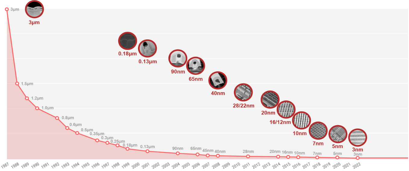
Process nodes are a specific generation of semiconductor manufacturing technology. They're historically distinguished by the dimensions of the minimum transistor size that they can create. In the past, this used to be very straightforward - as late as the 90nm node, transistors were indeed the dimensions advertised. 90nm meant 90nm. Today, the leading edge node is 3nm, but the transistors are fucking 20-25nm wide. It's bullshit. So whatever, name it whatever, some smaller number, doesn't matter. It's better, smaller, faster, that's all that really matters. Complete semantic collapse, who cares anymore? Intel calls theirs Angstrom - LOL. TSMC should call their next node "1 Planck" and just banish this absurdity forever. Maybe then they'll take naming privileges away from the nerds. Actually now that I think about it, it sounds like that's exactly what happened after 90nm, but instead of letting someone smarter and more tasteful name the process nodes they gave it to the worst people... marketing.
Ok, rant over.
Yields
Another important concept to understand about modern semiconductor manufacturing is yields. Yield refers to how much of a chip or wafer is functional at the end of the manufacturing process. No manufacturing process is perfect, and there is always some defect rate. But for modern integrated circuits, this is true to the extreme: because of the absurd precision and thousands of process steps required, every wafer contains defective dies. This might be because of slight misalignment during the lithography step, or a contaminant dust particle landing on wafer, or some minor seismic activity.
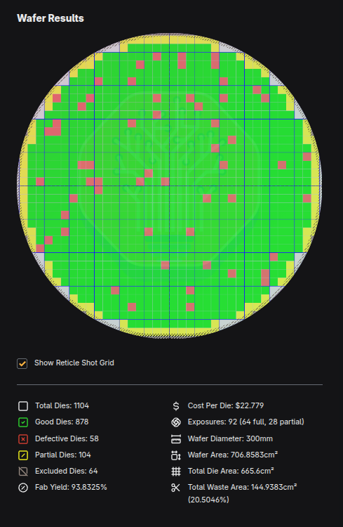
When a new process node is being developed, initial yields can be as low as 50%. Engineers and technicians then work to eliminate any sources of persistent defects, often driving yields up to 80-90% over time. The rate at which yields can be improved is directly related to the scale of production - the more chips produced, the faster defect sources can be identified, the faster they can be remedied, and the more certain you can be that the solution actually addressed the root cause. As such, a core part of the foundry business model (which TSMC helped to pioneer, and which will be discussed in greater detail later in this piece) is scaling process node production extremely rapidly from beginning in order to accrue these yield gains as rapidly as possible. Achieving high yields as a process node matures is crucial to the economic viability of foundries.
Process Steps (in Detail)
Now that we've covered many of the core concerns of semiconductor manufacturing, it's time to dive into the process in more depth and understand the various individual steps, their roles, and the companies that supply the equipment.
Material Modification
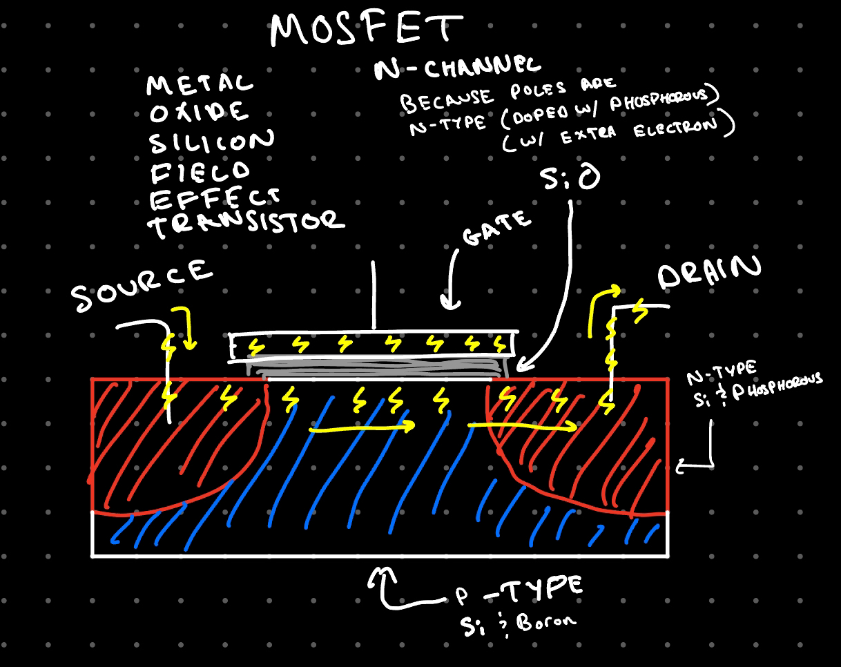
Material modification is almost entirely a FEOL step, as it's the method by which transistors are created. These transistors form the base layer of ICs, upon which layer on layer of interconnects, vias, and SiO2 are added. By implanting ions (typically Phosphorous or Boron) into the silicon lattice of an otherwise blank wafer, conductive areas are placed, forming the foundation of transistors. Ion implantation causes some atomic damage to the wafers, so annealers (machines that heat and cool the wafer to reform/heal the silicon lattice) are required after the wafer is doped.
Ion Implantation
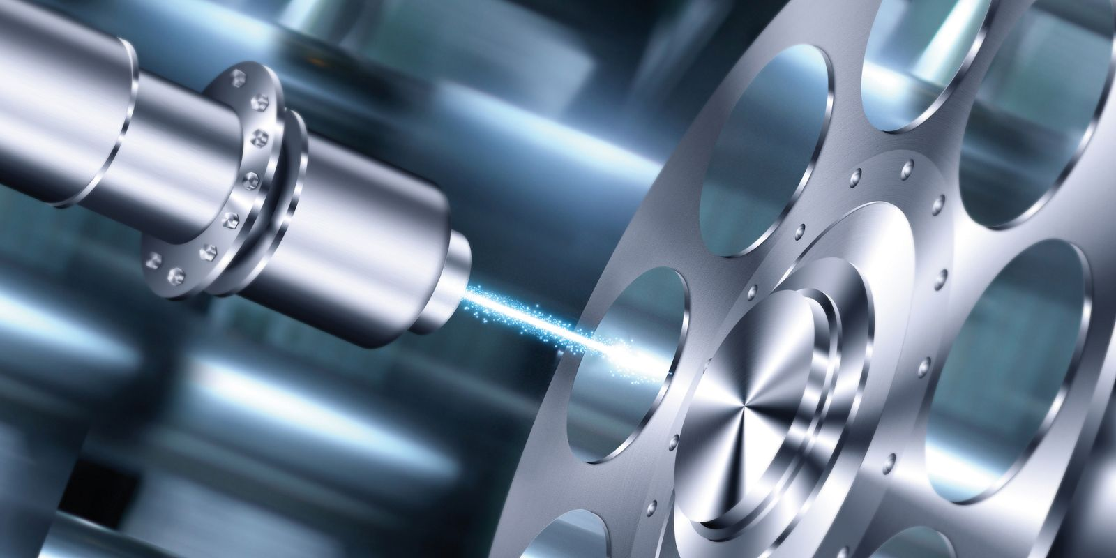
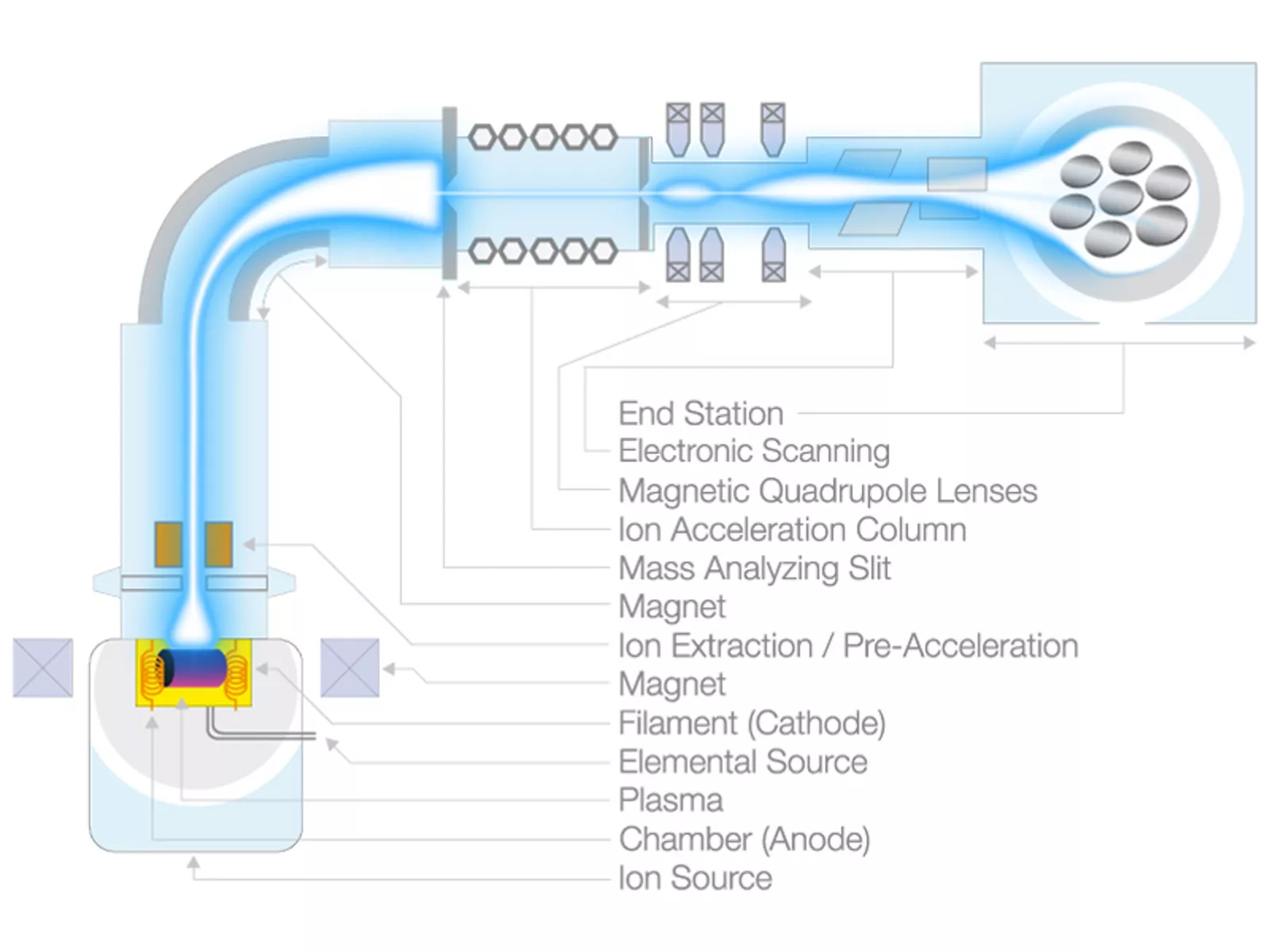
Ion implantation is done by shooting a controlled, high energy plasma ribbon of Boron or Phosphorous ions into the wafer at precise locations. Generating and controlling this plasma ribbon requires immense energy and sophisticated electromagnets. While not as complex as EUV lithography, ion implantation is remarkably involved.
Ion Implantation Equipment Manufacturers
Applied Materials (AMAT)
- Exec Summary: Ion implantation, CVD & PVD, etch, CMP, metrology/inspection, advanced packaging US machine maker
- Scale: public, 35k employees, $27bn rev, $140bn mcap
- Notes: Second largest fab equipment manufacturer behind ASML, accounting for 20% of total equipment spend. They account for 60% of the ion implantation market (Varian), 50% of the CVD market, 60% of the PVD market, 16% of the etch market, 40% of the CMP market, & 15% of the metrology/inspection market. 40% of their revenue comes from advanced nodes (<=7nm) and the remaining 70% from ICAPS (>=28nm). By covering a wide breadth of process steps, and providing integrated/platform level support across all those processes, AMAT presents a very compelling value proposition especially at leading edge nodes where substantial fine-tuning and customization are necessary. They sell into TSMC, Samsung (Foundry & Memory), Intel, SMIC (and other Chinese fabs), SK Hynix, and a number of trailing node customers. No single customer dominates their sales.
- Location: HQ in Santa Clara, CA, manufacturing in TX, MA, Singapore operations center, offices globally (none in china)
- Tags: us, fab, machines, ion implantation, cvd, pvd, etch, cmp, inspection, packaging, feol, mol, beol
Axcelis Technologies
- Exec Summary: US ion implantation machine pure play
- Scale: public, 1500 employees, $1bn rev, $2.2bn mcap
- Notes: Mature node single wafer ion implantation machine pure play that accounts for 20% of the overall ion implant equipment market (second behind ASML). Most of its revenue comes from mature nodes, with only about 10% coming from leading edge nodes. All revenue comes from ion implantation equipment
- Location: HQ in MA, US, with logistics center in SK
- Tags: us, fab, machines, ion implantation, feol
Material Addition
Material addition is largely a MOL step - new layers of silicon, interconnects, and vias are all added in each layer of the chip, requiring a handful of specialized tools. The primary objective here is placing tiny amounts of materials with high precision, in a thin, uniform layer across the entirety of the wafer. Depending on the aspect ratio of the features being created and the materials being added, there's a couple different methods.
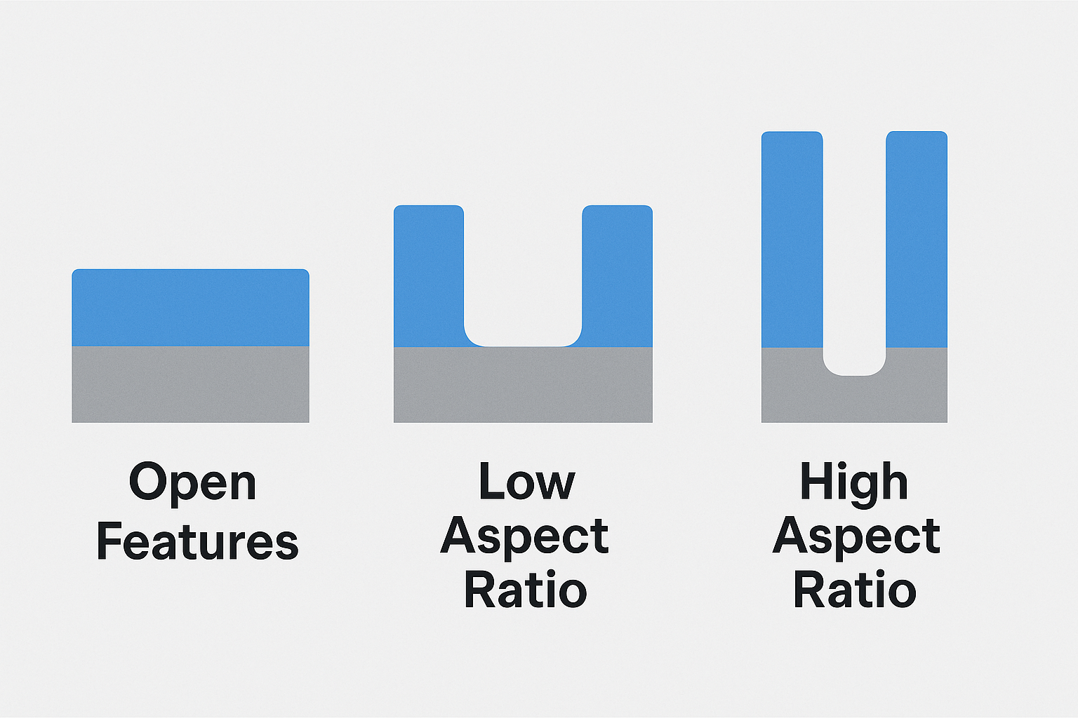
On a high level, as aspect ratios increase (features get narrower and deeper), finer control is required to ensure that material is added exactly where its needed - namely in the trenches at the bottom of features, which are the most difficult part to reach.
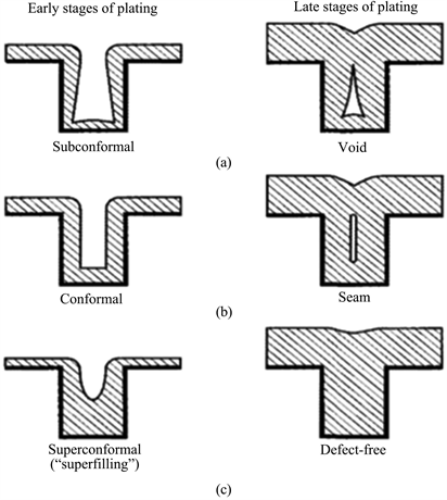
PVD is used for lower aspect ratio features like interconnects, CVD is used for medium aspect ratio features like vias, and ALD is used for the highest aspect features like FinFET trenches.
The same handful of companies dominate all of these process steps, and that's to be expected - they're quite similar, and share many of the same technical challenges. I've included the companies at the very end of this section to avoid repetition.
Physical Vapor Deposition (PVD)
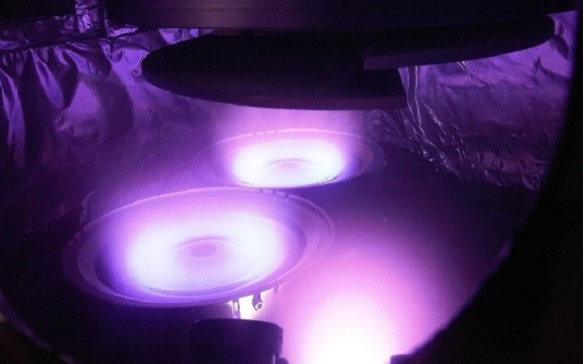
PVD is used to apply thin layers of metal to form interconnects across the entire surface of the wafer. This is most often accomplished via 'sputtering', where a metal source is bombarded with electrons in a vacuum, creating a directed plasma flow which builds a very fine film-like deposition layer of atoms on the negatively charged wafer target. For NVIDIA GPUs, metals such as Copper, Tungsten, Cobalt, Tantalum, Nickel, and Hafnium are used at various stages with this method.
Chemical Vapor Deposition (CVD)
CVD is a more finely controlled deposition process, and is used to fill deeper features than PVD and also provide a cap layer on higher aspect ratio features on more advance nodes that can then be bulk filled by PVD - CVD ensures the finer details of the feature are properly filled, then PVD can handle the remaining voids.
Atomic Layer Deposition (ALD)
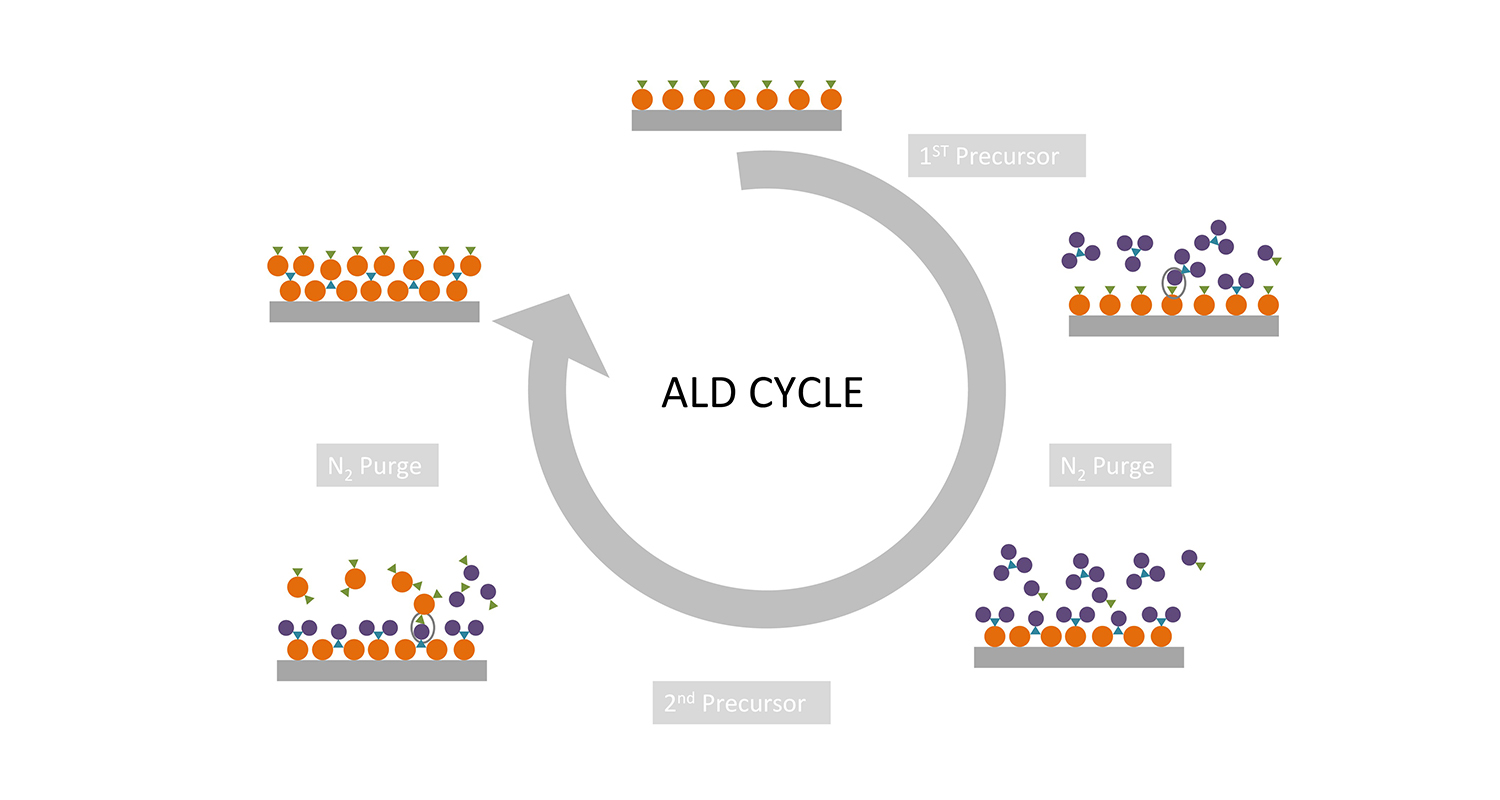
ALD is a specific type of CVD that is atomically precise, and it's achieved by using very specific gas procedures. ALD is used for the smallest, highest aspect ratio features, and has increasingly aggressive adoption at the leading edge nodes. ALD is also the slowest deposition method, as it requires a number of discrete gas steps to create its atomic layer, so it's not feasible for use in MOL (yet).
Epitaxial Growth (Epi)
Epitaxial growth is a crystal growth process. Epi is used to build up a blank layer on a wafer to begin a new cycle, and is similar to deposition steps in outcome, in that it seeks to add a thin, even layer of SiO2 to the wafer on top of the existing layer, but does so by growing a crystalline layer (instead of a metallic one).
Material Addition Equipment Manufacturers
ASM International
- Exec Summary: Leading edge node deposition equipment manufacturer
- Scale: public, 4.5k employees, $3.2bn rev, $27bn mcap
- Notes: Market leader in atomic layer deposition equipment with 55% mshare and major player in epitaxy with 20% mshare. Growing rapidly, with a focus in GAAFET. Almost all of their revenue comes from leading edge nodes (75%). Very high margins.
- Location: HQ in NL, manufacturing in Singapore & SK, R&D labs in EU, JP, SK, & US.
- Tags: fab, machines, nl, cvd, ald, depo, advanced
Applied Materials (AMAT)
- Exec Summary: Ion implantation, CVD & PVD, etch, CMP, metrology/inspection, advanced packaging US machine maker
- Scale: public, 35k employees, $27bn rev, $140bn mcap
- Notes: Second largest fab equipment manufacturer behind ASML, accounting for 20% of total equipment spend. They account for 60% of the ion implantation market (Varian), 50% of the CVD market, 60% of the PVD market, 16% of the etch market, 40% of the CMP market, & 15% of the metrology/inspection market. 40% of their revenue comes from advanced nodes (<=7nm) and the remaining 70% from ICAPS (>=28nm). By covering a wide breadth of process steps, and providing integrated/platform level support across all those processes, AMAT presents a very compelling value proposition especially at leading edge nodes where substantial fine-tuning and customization are necessary. They sell into TSMC, Samsung (Foundry & Memory), Intel, SMIC (and other Chinese fabs), SK Hynix, and a number of trailing node customers. No single customer dominates their sales.
- Location: HQ in Santa Clara, CA, manufacturing in TX, MA, Singapore operations center, offices globally (none in china)
- Tags: us, fab, machines, ion implantation, cvd, pvd, etch, cmp, inspection, packaging, feol, mol, beol
Masking
Many textbooks can be (and have been) written on masking, EUV, and the countless complexities of this single step. Indeed, I'm quite certain I could spend a lifetime attempting to fully understand this process step and still have much to learn. I'll try to cover the most important points, but be warned that this area in particular has a near limitless knowledge cap.
Masking is the process by which a template/blueprint/stencil for a layer is transferred from a source design onto the wafer. In the case of EUV lithography, which is the process used at leading edge nodes, colossal machines generate extreme ultraviolet light by shooting a huge laser at drops of molten tin, then bouncing, transforming, and refocusing that light to expose a precise pattern on a wafer. By transferring this pattern from mask to wafer, the pattern can then be used to remove material on the wafer with precision and speed.
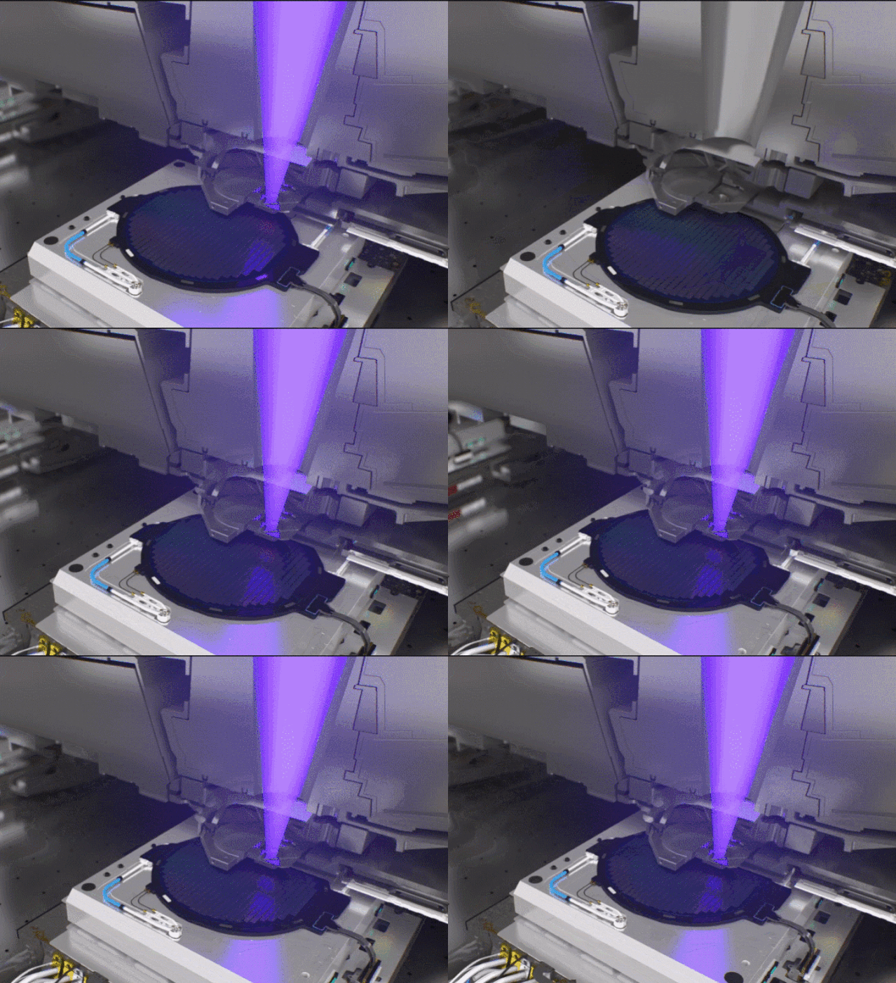
Masking is the most crucial step in modern SM. It is the most expensive step - ASML's EUV machines typically cost $150m and consume immense amounts of energy while running. Its technology is by far the most complicated and monopolized of all of the process steps - only ASML makes EUV machines used on leading edge nodes. And it's the bottleneck step - feature size, yield, and wafer process speed are all determined principally by the capabilities of these masking machines. This has been the case for quite some time - it's likely that improvements to lithography have driven the bulk of Moore's Law since the 90nm node, and attributable improvements have only slowed recently as gate width has begun to approach the fundamental lower limit of this paradigm.
ASML
To understand masking, lithography, and modern semiconductors, we must understand ASML. Here's the top line overview of the Dutch company for context:
- Exec Summary: Sole producer of lithography machines required to produce leading node ICs
- Scale: public, 44k employees, $30bn revenue, $308bn mcap
- Notes: ASML is the semiconductor lithography company, with a monopoly on EUV and a near monopoly on immersion DUV, they account for ~90% of the lithography market for sub 90nm process nodes
- Location: HQ in Veldhoven, NL, optics in CT, USA & Berlin, DE, subsystem & service hubs across the world
- Tags: fab, litho, euv, duv, nl, monopoly
But there's much more to know about ASML. First, it's important to understand that ASML is primarily a systems integrator, which is to say that while they design, construct, qualify, and service their lithography machines, they source almost every subcomponent from a staggeringly long list of external suppliers. Of their hundreds of suppliers (some estimate over 700 tier 1 suppliers), below are some illustrative examples of the most critical tier 1 suppliers and subsystems. By getting a feeling for these suppliers, you'll also begin to understand how ASML's EUV machines operate.
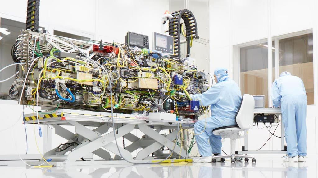
Laser - Trumpf
The first part in the chain of steps that results in a complete pattern projected with EUV light on the wafer begins with an extremely powerful laser that's supplied by just one company.
- Exec Summary: Laser & Machine tool group
- Scale: private (family owned), 19k employees, $5.5bn rev, ? mcap
- Notes: Industrial machine tooling and high powered laser manufacturer. One of the largest suppliers of industrial laser machines in the US and abroad. Sole supplier of ASML EUV drive lasers. SM accounts for 20% of the business
- Location: HQ in DE, manufacturing throughout EU, co-located with ASML for EUV integrations
- Tags: de, fab, subcomponent, litho, asml, laser, monopoly
This high power laser is used to generate EUV light by vaporizing tiny tin droplets, and it's this vaporization that in turn releases the 13.5nm wavelength EUV blast that does the important lithography work. Each EUV blast is actually separated into 2 separate laser pulses - the first is a low power preparatory shot that deforms the spherical tin droplet into a thin disk so as to maximize surface area and increase the vaporization rate of the tin. Once the molten tin disk has been prepared, it's blasted with the high power pulse, and it's this pulse that vaporizes the tin. This high power pulse is tens of kilowatts in strength, and happens 80,000 times a second, with each blast targeting a new tin droplet.
Complete Light Source - Cymer (subsidiary)
Next, these lasers are combined with the tin droplet generator to create the complete EUV light source. Cymer, acquired by ASML in 2013 for 2.5bn, is the company that does this integration.
- Exec Summary: Designer and builder of laser/tin-plasma EUV and DUV light sources
- Scale: subsidiary of asml, 1k employees, 500m rev, ? mcap
- Notes: Designs and builds light sources for all of ASML's lithography machines.
- Location: HQ in CA, US
- Tags: us, fabs, subsidiary, asml, laser, litho
Macro Optics - Carl Zeiss
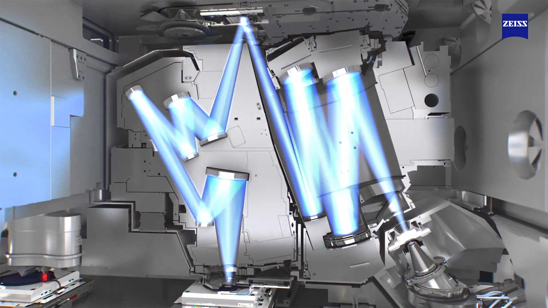
Now that the EUV light has been generated, we need to focus & direct it to the reticle (and then the wafer). This is where the mirrors come in. Once again, only a singular company is capable of producing these mirrors
- Exec Summary: Sole EUV Optics manufacturer for ASML
- Scale: private, 46k employees, $11.4bn rev, ? mcap
- Notes: Produces 100% of EUV optics and 80% of DUV optics. Tight partnership with ASML. ASML holds a 25% minority stake. Growing business in e-beam metrology.
- Location: HQ in DE, global footprint
- Tags: de, fabs, euv, litho, asml, optics, metrology, inspection
These mirrors have to be essentially perfect - they are one of the true limiting steps of EUV lithography, as feature precision and light transfer are bottle-necked in no small part by the construction of these optics. Zeiss goes to great lengths to ensure they are perfect, even down to an atomic level. They're constructed from numerous layers of material to tightly control the reflective properties, and ensure as much of the source light is transferred to the wafer. Despite this, only about 70% of the EUV light survives each mirror bounce. This is because EUV light is absorbed by basically everything - solids, gases, glass, air, etc. Less than 1% of the source light ever reaches the wafer. This should illustrate why these mirrors are so important.
Patterning - Reticles
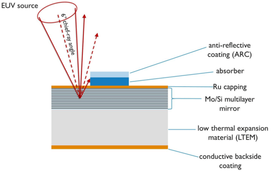
Reticles contain the essential pattern that is then projected onto the wafer. In other (older) lithography processes, this information was transferred via a mask - think of a stencil sitting atop the wafer, mapping out positive and negative exposure areas, with light shining through directly to the wafer. In this case, the reticle is actually a mirror, but it only selectively reflects light so as to create its desired pattern. Each layer in an IC has its own reticle photomask, and given that there can be 80 layers in modern ICs, that means a lot of unique masks.
Blank, atomically perfect multilayer mirrors are painstakingly built up layer by layer (namely alternating Molybdenum & Silicon layers for maximum reflectivity, remember the Zeiss mirrors). These blanks are then patterned/inscribed with an ebeam, a process which can take multiple days depending on the complexity of the layer. Then the reticles are closely inspected and mounted.
Precision matters even more here than at any aforementioned process step, if that is imaginable - the reticles are the sole information source in some important sense, and its their pattern that is beamed over and over upon millions of wafers. These are some of the most pristine and perfect objects in the universe.
Reticles are typically manufactured by the foundries in close coordination with WFE manufacturers and the end client. TSMC has its own reticle manufacturing process, as does Samsung and Intel.
Defect Prevention - Mitsui Chemical
Sitting in front of the reticle is a protective film called a pellicle - this pellicle acts as a physical and optical shield, in that it stops any particulates or contaminants from landing on the reticle, and by catching those particulates outside of the focal plane of the reticle, limits or completely eliminates their possible impact on the EUV pattern. These films also have to transmit most of the EUV light that hits them, which is a challenge because (as previously mentioned) everything absorbs EUV. Mitsui is the only company in the world that manufacturers these pellicles.
- Exec Summary: Large chemical co with critical T1 euv pellicle subdivision
- Scale: public, 17k employees, $11.8bn rev, $3.9bn mcap
- Notes: Sole manufacturer of ultrathin EUV pellicles used in ASML EUV machines. SM activities account for <10% of overall revenue, but are very profitable and growing rapidly (30-40% YoY).
- Location: HQ in JP, manufacturing in TW, KR, & SP
- Tags: jp, fab, subcomponent, euv, litho, asml, monopoly
Wafer & Reticle Mechatronics - ASML Berliner (Prev. Berliner Glas)
Both the wafer and the reticle (mask) have to be both moved and held in position with extreme accuracy. ASML Berliner (previously Berliner Glas) is the only company that manufacturers the wafer and reticle platforms/tables (commonly referred to as 'chucks').
- Exec Summary: Subsidiary of ASML, EUV subcomponent manufacturer
- Scale: private (subsidiary), 1.7k employees, $350m (?) rev, ? mcap
- Notes: Acquired by ASML in 2020 (for 260m?). Sole manufacturer of precision wafer and reticle chucks among other high precision components of EUV machines.
- Location: DE
- Tags: de, subcomponent, fab, euv, litho, asml, monopoly
Other Mechatronics - VDL Enabling Technologies Group (ETG)
Positioning/moving wafers within the EUV machine requires just as much precision as every prior step - VDL, a private Dutch company, manufacturers most of these components (like the wafer handler) in close cooperation with ASML. VDL also supplies these mechatronics to a wide range of other WFE manufacturers in addition to ASML.
- Exec Summary: Precision mechatronic module builder for lithography
- Scale: private (family owned), 5k employees, 2bn rev, ? mcap
- Notes: Supplies the entire WFE market with precision mechatronics - wafer handlers, wafer chambers, vibration-isolated columns, etc. 80% of sales are linked (directly or indirectly) to leading edge fabs. Accounts for a large portion of mechanical content of ASML EUVs. Also sells into AMAT, Lam, ASM, KLA.
- Location: HQ in Eindhoven, NL, manufacturing in CH, US (FL/CA), CN, SP (new megafactory), VN
- Tags: nl, fab, subcomponent, mechatronic, euv, litho, asml, wafer, amat, lam, asm
This is just the beginning of a long list of suppliers and subcomponents that can be found in one of ASML's EUV lithography machines. They are likely among the most complex physical objects mankind has ever created. Even the logistics of transporting finished systems from ASML's HQ in Veldhoven to their destination foundry would justify a hefty book to exhaustively examine. For any sort of practical understanding, we must be satisfied in this case with what on almost any other topic might be considered a gross oversimplification.
Material Removal
There are two primary types of material removal steps, and each serves a unique purpose - etching and planarization.
Etching
Etching can be done either with high energy plasma or chemically, however at leading edge nodes it's primarily the former.
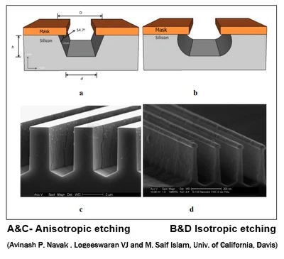
Plasma etching typically occurs directly after the masking step is complete, and removes exposed SiO2 material so as to create the required channels for interconnects and vias. Because plasma flow can be directed electromagnetically with high precision (it's anisotropic), it's the ideal method for carving out predictable and directed voids in previously masked material.
On trailing nodes and on some specific (and not high precision steps) in current mature nodes, chemical etching is used as it's much faster and cheaper. But for fine features, chemical etching is no longer used because it's isotropic:
The leading etching equipment manufacturers have (largely) been discussed in depth in other previous sections: Lam Research, Applied Materials, and Tokyo Electron are dominant in this area, each with their own specific niche.
Tokyo Electron (TEL)
- Exec Summary: WFE manufacturer for etch, depo, clean, track, inspection, etc with a monopoly on photoresist application/development process step
- Scale: public, 20k employees, $15bn rev, $68bn mcap
- Notes: Has huge mshare (maybe 100% in EUV?) on photoresist coater/tracker/developer process step, substantial presence in plasma etch and deposition (10% mshare each), wet cleaning, & wafer probers/banding. Is the third largest WFE manufacturer behind Advanced Materials and Lam with about 12% overall mshare. 70% of TEL's revenue come from leading edge node processes, with the remaining 30% attributable to legacy, trailing nodes.
- Location: HQ in Tokyo, US HQ in Austin, global sales, distribution, and support network.
- Tags: fab, wfe, photoresist, litho, jp, etch
Planarization
Planarization occurs near the beginning of a new layer cycle to ensure that the newly added blank SiO2 layer is perfectly flat and at the target thickness. This is is achieved through a process called Chemical Mechanical Planarization (CMP), which is essentially super precise grinding of the wafer face. Various chemicals and slurries are needed to grind wafers without creating defects from friction. Applied Materials is the primary equipment manufacturer in this domain as well, followed closely by Ebara and TEL.
Metrology/Inspection
Inspection involves scanning the wafer for any uncaught issues so as to potentially remedy or work around them, and also to prevent a faulty process step from introducing issues into other wafers. While possibly not as glamorous as lithography or plasma etching, inspection is essential to driving improvements in yields by preventively correcting and identifying the sources of defects. Given the physical complexity of the wafers, this is a nontrivial task involving petabytes of data which are then closely analyzed and used to make realtime corrections to process steps. The inspection equipment market is dominated by a single US firm, KLA:
KLA
- Exec Summary: Largest supplier of inspection/metrology WFE
- Scale: public, 15k employees, $10bn rev, $118bn mcap
- Notes: KLA is the inspection tooling company. KLA has an 80% mshare in optical patterned wafer inspection, and 60% mshare in process control market. About 80% of their revenues come from new machine sales, and 20% comes from servicing existing machines. They primarily manufacture optical and ebeam wafer inspection tools, reticle inspection, and process sensors. KLA also supplies comprehensive software to analyze and correct defects.
- Location: HQ in US (CA) manufacturing in US, UK, IS
- Tags: us, fab, wfe, inspection, metrology, monopoly
While increasingly true of most process steps, inspection is a domain where software is becoming paramount and a primary driver of improvements. Modern foundries now generate immense amounts of data (think high speed video and super high definition scans and photographs) about each wafer at each process step. This data is then analyzed and used to modify and fine tune future process steps, tailoring the production of each individual wafer so as to maximize yields. KLA has a substantial advantage in this regard, as its current hardware monopoly has allowed it to build a colossal historical dataset that in turn gives it a durable software moat.
Cleaning
Despite being last on this list, cleaning steps are actually among the most numerous process steps. After almost every other step, the wafer is cleaned. This typically involves spincoating the wafer in ultrapure water or isopropyl alcohol (IPA) to rinse away any contaminants on the surface. Water used to clean wafers needs to be ultrapure because it cannot leave behind any residue once it's been evaporated. Ultrapure water is so contaminant free that it's mildly toxic to consume (most water has some amount of naturally occurring minerals and ions).
Cleaning has a few more competitors than other pther process steps, but it's still dominated by a handful of (mostly) previously mentioned firms, namely TEL & Lam Research. The largest player in the space, however, is the unmentioned SCREEN Holdings:
SCREEN Holdings
- Exec Summary: Wafer cleaning WFE pure play
- Scale: public, 6.4k employees, $4.2bn rev, $7bn mcap
- Notes: Has the largest mshare in post-litho photoresist strip & particle/metal removal between EUV, etch, & CMP steps (>60% mshare). 40% of their sales are to leading edge node processes.
- Location: HQ in JP, Manufacturing in JP, global service centers.
- Tags: jp, fab, cleaning, litho, photoresist
Scale & Statistics
Most of the revenue is in nodes from 90nm onwards (mature and advanced). TMSC doesn't even touch older nodes (TSMC's node pricing strategy, among other business model innovations, will be discussed later in this piece). The advanced/leading nodes are used for CPUs, GPUs, AI accelerators, and various forms of memory. Moving towards the older, more mature nodes, applications shift to automotive ICs, sensors, and IoT chips. As a rule, leading nodes make up the vast majority of revenue and profits.
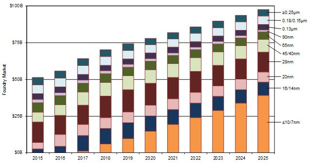
To get a better idea of the scale, profitability, and various revenue sources of the biggest players in the space, see the following quarterly aellagrams.
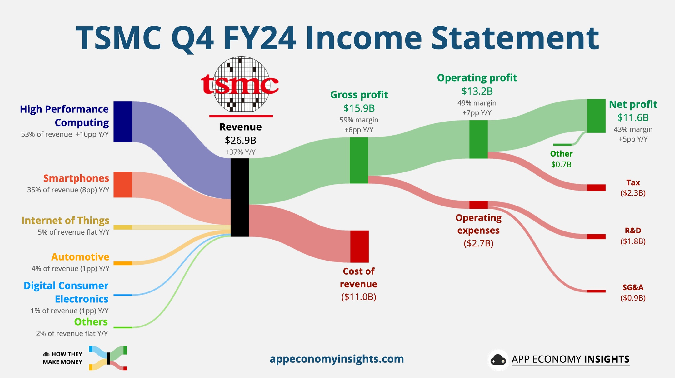
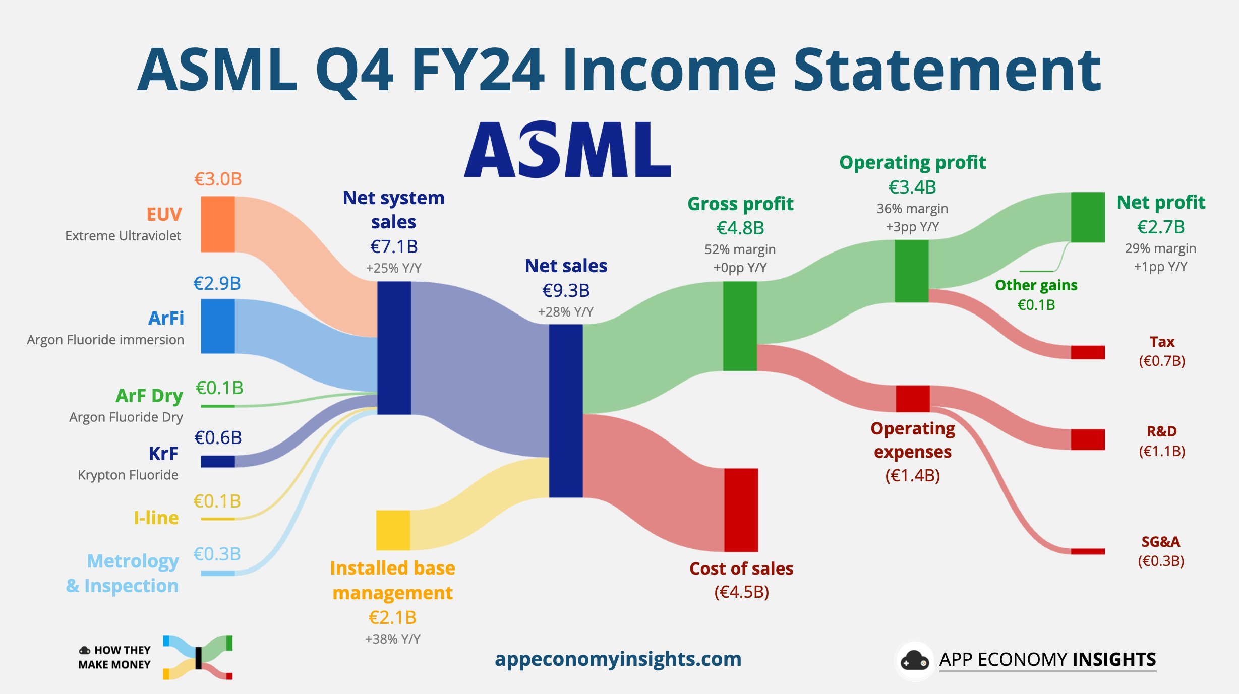
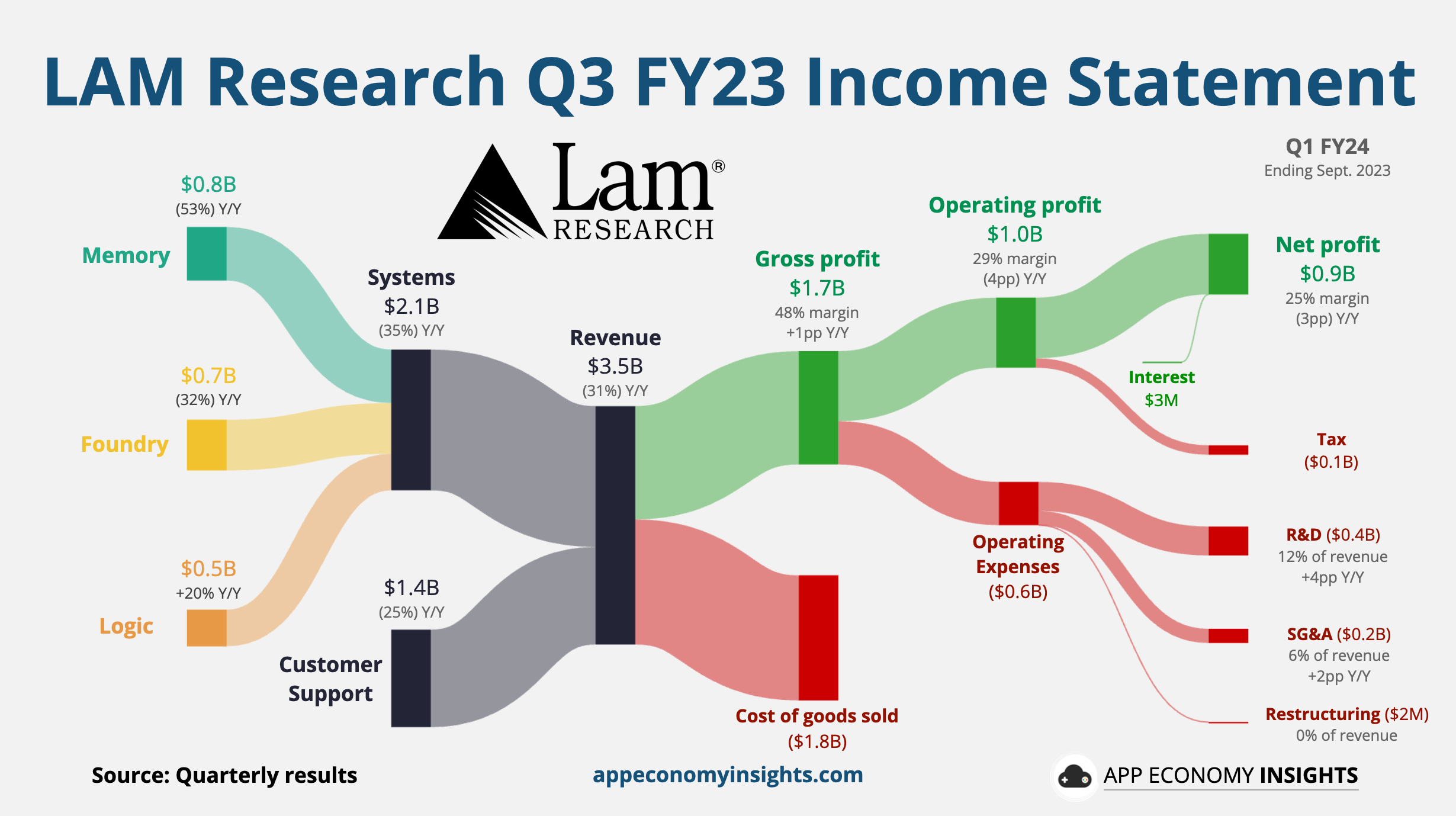
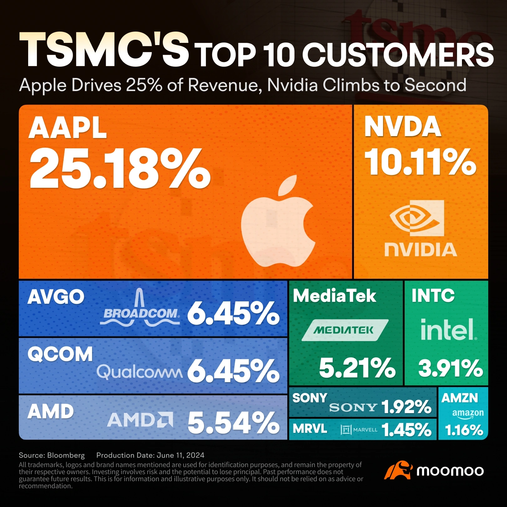
TSMC's largest customer is still Apple, with NVIDIA as a distant second. One must imagine that in the case of AI takeoff, consumer electronics will (probably) represent a much smaller proportion of overall compute sales than they currently do.
Business Model Innovation
One key innovation in semiconductor manufacturing lies not in the technology itself but in a secular trend in business models among the leading players in the space - while vertical integration is often heralded as a key step in a maturing business model, the heavyweights in semiconductors seem to be doing the opposite - specializing in a singular step or domain and shedding all other business lines. Why has TSMC outperformed Intel? Why is there no competitor for ASML? While there's lots of potential answers, one compelling explantation lies in R&D spend - given the exponentially increasing complexity and capital costs of processes at leading edge nodes, it seems distinctly possible that fragmentation of revenue, and by extension R&D spend, represents a fundamental roadblock to developing the next node. Furthermore, ensuring that you don't compete with your customers may be the only way for them to become comfortable with you monopolizing a particular step in the semiconductor supply chain.
Most of the monopolies and semi-monopolies in this space exhibit this behavior - ASML, Applied Materials, Lam, KLA, TEL, etc are not working towards building their own foundry businesses. TSMC is not building a consumer chip design arm. Vertical integration, a strong trend in most industries, has seemed largely counterproductive in the world of semiconductor manufacturing. It may be that the capital intensity of these businesses all but requires singular process step focus. It may be that competitive dynamics between supplier and customer shrink the TAM of vertical integrators sufficiently to eliminate their scale and profitability. Whatever explanation is most plausible, it's important to reckon with this fact: vertical integrators are not the current winners in business of semiconductor manufacturing.
Foundries
Foundries are where all of the aforementioned tools and technologies are brought together into a single production line, into which blank wafers, metals, gases, ultrapure water, and immense energy are poured, and out of which finished ICs are shipped. Foundries are the ultimate system integrators, purchasing and finetuning equipment for every process step (in close coordination with their suppliers) to produce the chips designed by their customers.
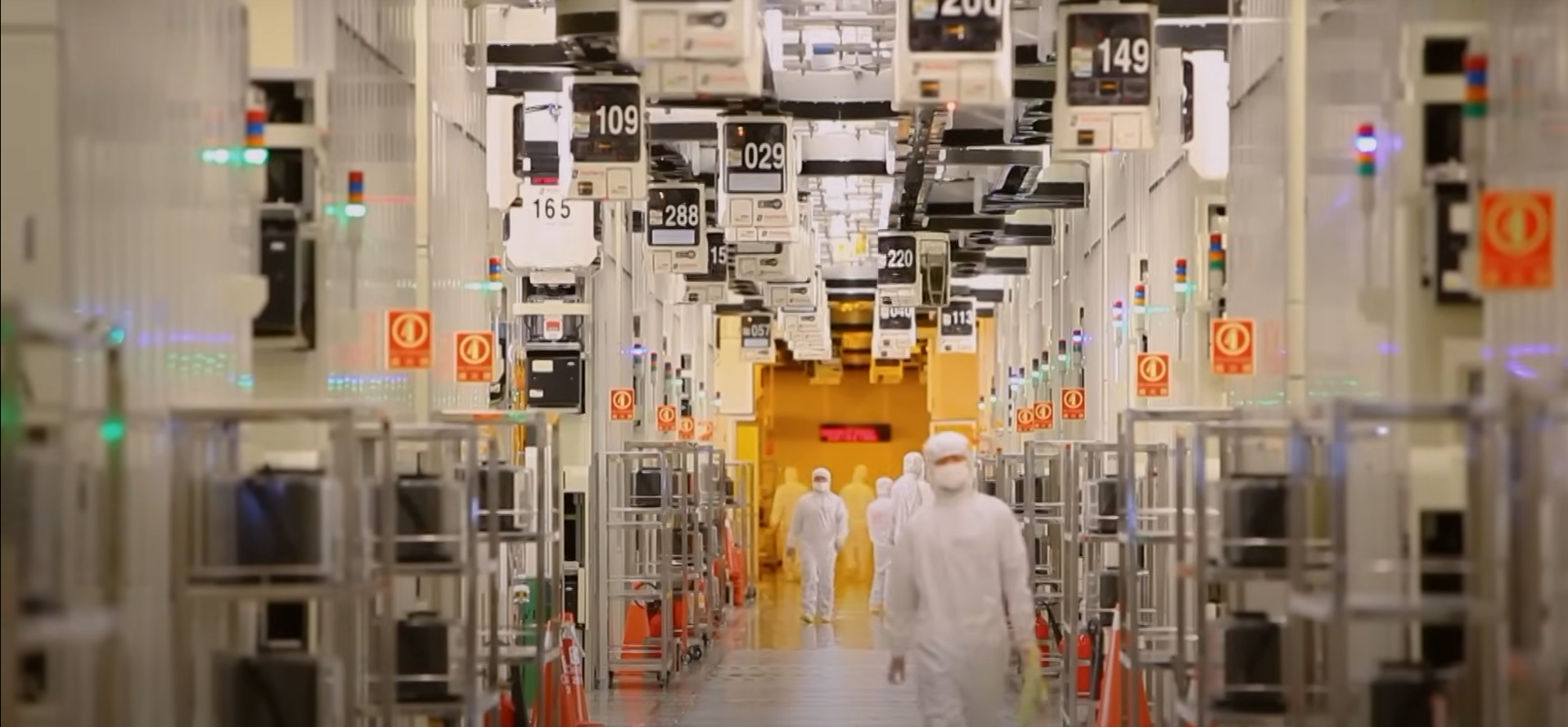
The story of the modern day foundry is a story of a small handful of massive players. Most importantly, it's the story of Taiwan Semiconductor Manufacturing Company (TSMC), the behemoth that has come to dominate the market.
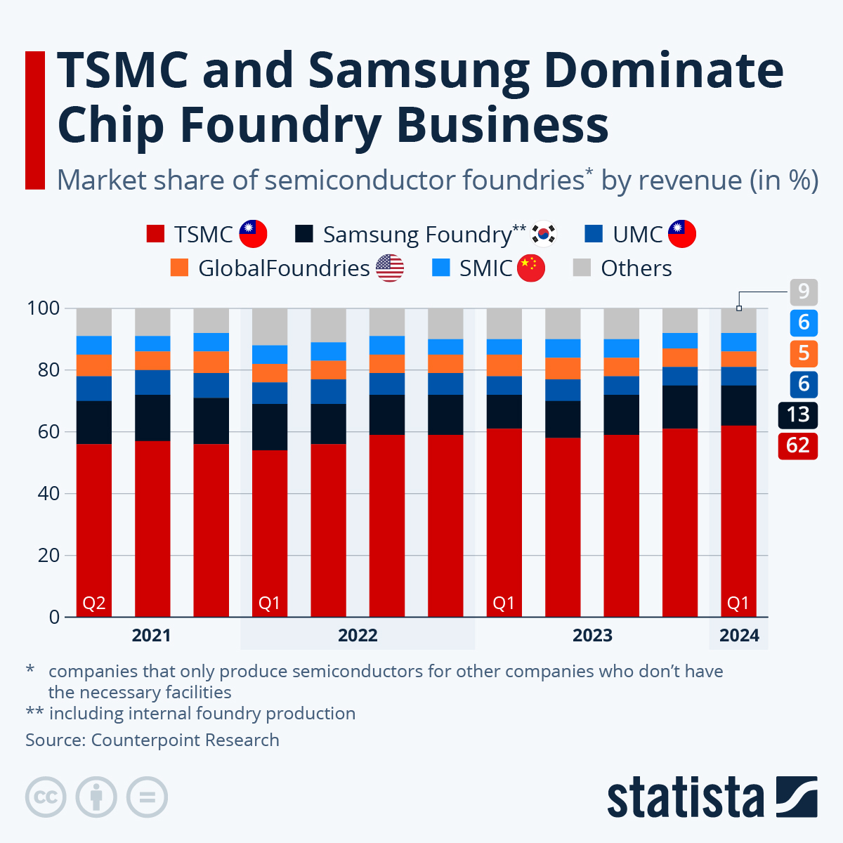
TSMC
- Scale: public, 84k employees, $90bn rev, $1.18tn mcap
- Notes: Accounts for 65% of the global foundry market, 90% of 3nm & 5nm, and 70% of all <=7nm process nodes. 70% of revenue comes from leading nodes (<=7nm). Has recently constructed/begun construction on a number of global fabs in the US, Japan, & Germany.
- Location: HQ in Hsinchu, TW, with global foundry footprint.
- Tags: tw, us, jp, de, fab, monopoly
Much like ASML, whole books have been written on TSMC. It may be that TSMC is the single most geopolitically important company in the world at the moment. When people in the industry talk about TSMC, it's with a mythological reverence: the astounding work ethic, the technological prowess, the visionary founder Morris Chang, the almost unimaginable scale of production. To understand semiconductors, one must understand TSMC.
Founded in 1987 as the first foundry pure play, Morris Chang (who had been snubbed for the CEO role at Texas Instruments) saw something that others didn't. First, advanced process nodes were becoming more and more capital intense. Second, fragmentation in the foundry market meant that most players were reticent to rapidly scale advanced node production. Third, the faster production was ramped on advanced nodes, the faster higher yields that could be achieved. What Morris Chang saw was a shift in the fundamental economics of semiconductor manufacturing: demand, capex, R&D would concentrate on the players who were willing to aggressively invest in and scale advanced nodes, and this in turn would give those players even more revenue to reinvest in advanced nodes, leading to a compounding and durable advantage.
Morris had come to understand this dynamic during his time at Texas Instruments. In possibly the first time that consultants have ever been useful, BCG proposed this "learning curve" pricing strategy where advanced nodes were priced much cheaper than what was at the time considered economically viable. This would induce demand and allow TSMC to scale production (and consequently yield) rapidly. TSMC has followed this strategy to a position of complete market dominance, aided by support from the Taiwanese government and deep technical talent pools.
Samsung Foundry
- Exec Summary: Second largest foundry
- Scale: subsidiary, 10k employees, $13bn rev, ? mcap
- Notes: Has 11% mshare of global foundry market. 40% of revenue comes from advanced nodes. Pioneer in GAAFET transistors. Major customers include Google, Tesla, & Facebook.
- Location: HQ in SK, SK & US fabs, some peripheral manufacturing in CN
- Tags: sk, fab, memory
Samsung is a distant second to TSMC, and has lost market share in recent years, but still represents a formidable player in the space. The Cheabol's foundry focuses more heavily on memory than TSMC, and has landed a long list of major customers including many of the US's tech giants.
UMC
- Exec Summary: Taiwan's other major pure play foundry
- Scale: public, 20k employees, $7.2bn rev, $19bn mcap
- Notes: 5% of global foundry revenue. Specialist focusing on mature and trailing nodes, with no capacity on 7nm and below. Hedge against geopolitical risk as it has mature fabs in TW, SP, CN, & JP.
- Location: HQ in TW (Hsinchu), mature fabs in SP, CN, & JP
- Tags: tw, sp, cn, jp, fab, trailing node
UMC differs from the previous 2 foundries in that it primarily focuses on mature and trailing nodes, and does so with great efficiency. The unfortunate reality is that trailing nodes are largely commodified, and as such the value and margin of the revenue from trailing node ICs is much lower than advanced nodes.
SMIC
- Exec Summary: China's pure play foundry
- Scale: public, 20k employees, $8bn rev, $59bn mcap
- Notes: 5% of global foundry market. Has a number of process nodes on 200mm wafers and 40nm - 20nm traditional nodes as well as a limited yield 7nm node using DUV multipatterning. Only 10% of revenue come from leading edge <=14nm FinFET nodes. Fabs across China.
- Location: HQ in CN, all manufacturing across CN
- Tags: cn, fab, trailing
SMIC is China's state backed semiconductor champion. ASML has been prevented from selling EUV lithography machines into China, and as such SMIC has had to get creative in pursuing advanced process nodes like 7nm - to pattern at these advanced nodes, SMIC uses DUV multipatterning (multiple passes with the longer 50nm wavelength DUV machines) to produce smaller feature sizes that would otherweise require an ASML EUV machine. This, however, drives down yields (think 10-30%) and consequently raises prices substantially. As such, SMIC's 7nm capabilities should be viewed as largely strategic in nature, and fundamentally uneconomical.
Founded in 2000 by Richard Chang (Zhang Rujing), SMIC's start is closely intertwined with TSMC: Richard had founded Shida Semiconductor in Taiwan, which was acquired by TSMC in 2000 for $5bn. Zhang was asked to stay on, which he did on the singular condition that TSMC would eventually construct a fab in mainland China. Upon learning that TSMC had no real plans for such a fab, Zhang promptly quit, giving up millions in stock options, and moved his entire family (as well as hundreds of engineers) to China to found SMIC. Zhang is presented as a singularly focused, maniacal semiconductor genius that singlehandedly built China's semiconductor capabilities.
GlobalFoundries
- Exec Summary: US foundry pure play
- Scale: public, 13k employees, $6.75bn rev, $21bn mcap
- Notes: 5% of global foundry revenue. Gave up on 7nm process node in 2018, so primarily manufactures trailing edge nodes for RF, IoT and other applications in aerospace and defense.
- Location: US HQ, fabs in US, DE, and SP
- Tags: us, fab
GlobalFoundries does not get as much coverage as other foundries on this list, however is by far the youngest fab mentioned having been founded in 2009. Baseload demand from US defense and aerospace contracts have given it a strong foundation to expand, but it has faced some setbacks on leading node production.
Intel
- Exec Summary: US integrated device manufacturer and fab
- Scale: public, 109k employees, $53bn rev, $98bn mcap
- Notes: Primarily manufactures CPUs for desktop (75% mshare), laptop (67% mshare), and server markets (70% mshare). Intel contract foundry only accounts for 1% of the global foundry market, but is strategic for their business. Leading edge nodes account for 45% of total revenue.
- Location: US HQ, manufacturing throughout US, IE, IS, DE (under construction)
- Tags: us, fab, idm, cpu
Intel is the one of the hallmark American technology companies. Much can be said about their immense early success, or their recent failures, but they cannot be counted out of the modern semiconductor and foundry business. They failed to capitalize on the contract foundry model, however much like GlobalWafers are well positioned to take advantage of geopolitical risk and turmoil as it arises.
Current Limitations & Design Frontiers
Let's talk about the Rayleigh criterion:
Critical Dimension (CD) = k1 • λ / Numerical Aperture (NA)
The Rayleigh criterion lays out the fundamental law governing transistor size at the moment - transistors can only be as small as the minimum feature size (or Critical Dimension) you can resolve. Let's delve a bit deeper into each variable here:
- k1 - In the classic slit aperture example of the Rayleigh criteria, k1 = 1 (and for a circular aperture, k1 = 1.22). This is for simple diffraction - if we employ some tricks, we can decrease k1 drastically beneath classic diffraction limits. For example, tuned photoresists produce a sharp binary boundary at otherwise continuous light gradients. By employing multiple such tricks, modern EUV machines reach k1 = 0.25.
- λ - Wavelength - Modern EUV machines use 13.5nm wavelength EUV light generated by tin plasma.
- NA - Numerical aperture is determined by the dimensions of the optics that focus the light. Current EUV systems have a numerical aperture of 0.33.
The name of the next generation of EUV machines should give a hint as to which variable ASML chose to optimize: 10-20 High-NA EUV systems have already been delivered and deployed to various fabs for pilot production. Intel received the first system in December 2023, with TSMC and Samsung taking delivery since. The sticker price for these systems is an eye-watering $400m, and each tool weighs 150-180 tons and requires 3 floors of fab floor space.
k1 and λ present myriad challenges to decrease. While some experimental demonstrations of k1 values approaching 0.2 exist, they are as of yet infeasible to implement at scale. As for decreasing wavelength beyond EUV (BEUV), power and vacuum sealing present the largest challenges. If you thought that 13.5nm EUV light was absorbed by everything, wait till you see 6.7nm BEUV light! None of these improvements are technically impossible. But they sure do sound difficult. One more feasible dimension of improvement is 3D transistor stacking: instead of arranging transistors in a single 2D plane, higher density can be achieved by constructing them in 3D. This is already done in memory.
Lithography is unequivocally the bottleneck step in modern semiconductor manufacturing. While there may exist another 1-2 generations of improvement that lie within the current lithography paradigm, it's eminently possible that alternative paradigms might have to be considered if a truly aggressive takeoff occurs.
Geopolitical Bottlenecks & US Dominance
I'm continually surprised by just how far behind China is lagging versus my previous perception of their relative ability. I fully expected to discover that SMIC was rapidly outpacing TSMC, and that (at least) trailing node production was dominated by the Chinese. Between Intel and GlobalFoundries, the US domestic foundries alone seem to have much greater capacity than the Chinese, and this is doubly true at the most advanced process nodes. Furthermore, I didn't expect to discover that between Applied Materials, Lam Research, & KLA, American firms dominate essentially all process steps outside of lithography.
There are undoubtedly some geopolitical bottlenecks that fall outside of the US's complete control: namely ASML & TSMC. It it unlikely (in my estimation) that we'll be able to construct a domestic ASML in a short enough timescale to matter. For TSMC, it seems that we could ultimately ramp up domestic production with great effort to replace some fraction of their current capacity on a 1-3 year timescale. But these are both largely moot points in my eyes: both of these firms and their respective countries of origin are very closely aligned with the US against China. ASML continues to adhere to US-imposed export restrictions on their EUV machines blocking their sale into China. Most of TSMC's largest customers are US multinationals. If China were to invade Taiwan, TSMC would cease to functionally exist, but this would only serve to slow down all players and alienate technical TSMC talent. The US holds colossal power over the current semiconductor supply chain, and Beijing can do little to change this in any reasonable time frame.