S2S 1: Inputs
Last Updated: 2025-06-18
Introduction
Understanding SI from first principles requires an understanding of its raw inputs. The current paradigm of modern semiconductor manufacturing is nearing atomic level precision, so we would be wise to understand the process with a perspective approaching that level of granularity. This piece covers those raw materials and primary inputs to semiconductor manufacturing in detail, explaining the purpose, source, and primary suppliers in the important categories. Finally, I close with an aside on rare earth metals.
Feedstocks
One of the defining characteristics of modern SM is the avoidance of impurities. The fabrication process is extremely precise, repetitive, and expensive, so small impurities are often amplified into disastrously expensive consequences. So while many of the base inputs for SM are (seemingly) widely available, most common sources are not economically usable as they're too impure. Take silicon, the most important substrate element - while Silica is one of the most abundant and easily accessible natural resources in the world, the level of purity required for certain components (like quartz crucibles used in the Czochralski process) eliminates almost every typical silica source, leaving only ultra high purity Silica from a single location - Spruce Pine, NC.
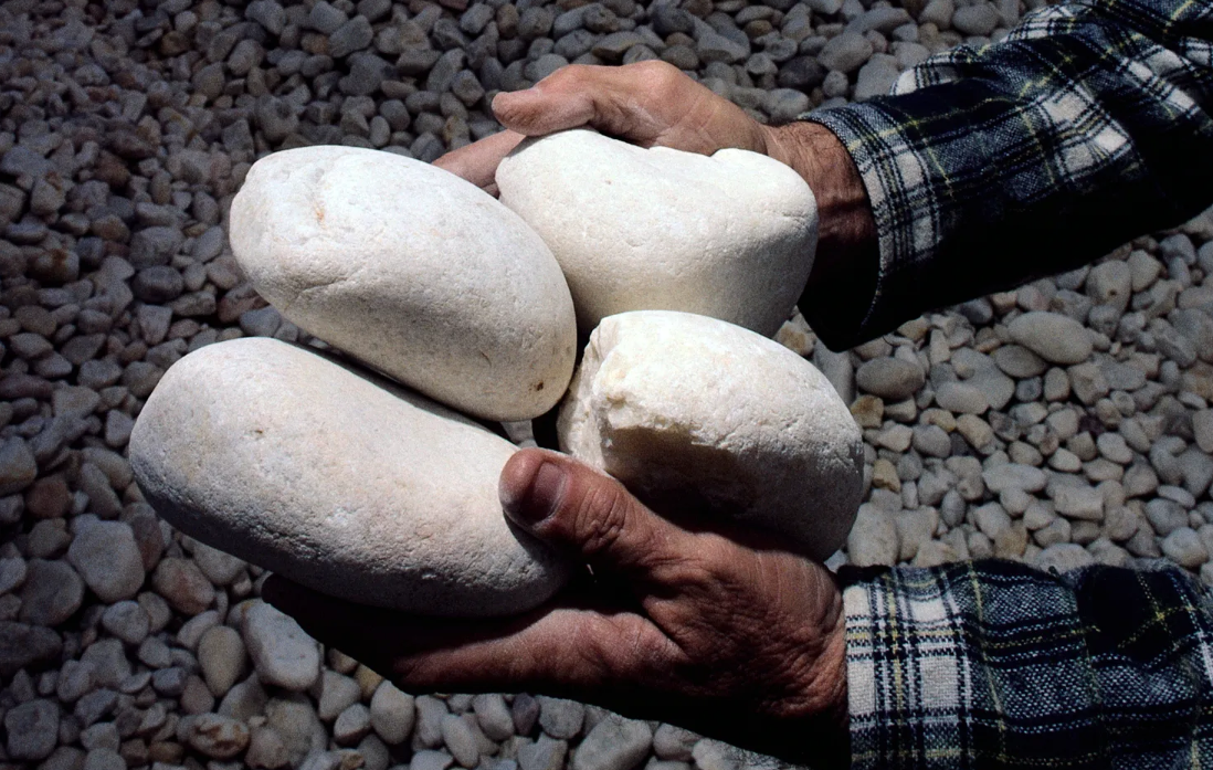
With this in mind, the following elements and inputs make up the bulk of the raw material feedstock of the semiconductor manufacturing process:
Detailed Inputs Table
| Category | Material | Application / Notes | Major Suppliers (Country, Market Share) |
|---|---|---|---|
| Substrate materials & ingot growth | Silicon (Si) | Dominant monocrystalline substrate for >90% of ICs | Wacker Chemie (DE, 35%), Hemlock Semiconductor (US, 30%), Tokuyama (JP, 15%), OCI Company (KR, 10%) |
| Germanium (Ge) | High‑speed/IR devices, multijunction solar‑cell substrates | Vital Materials (CN, 35%), 5NPlus (CA, 20%), Umicore (BE, 15%), Yamanaka Sangyo (JP, 10%) | |
| Silicon carbide (SiC) | Wide‑bandgap power electronics, high‑T applications | Wolfspeed (US, 40%), STMicroelectronics (FR/IT, 20%), ROHM (JP, 15%), ONSemi (US, 10%) | |
| Gallium arsenide (GaAs) | III‑V RF/microwave & optoelectronic devices | Freiberger (DE, 25%), AXT (US/CN, 20%), Sumitomo Electric (JP, 20%), IQE (GB, 15%) | |
| Indium phosphide (InP) | High‑speed photonic IC substrates | Coherent (US, 30%), JXNipponMM (JP, 25%), AXT (US/CN, 15%), Vital Materials (CN, 10%) | |
| Gallium nitride (GaN) | LEDs and RF power amplifiers | Wolfspeed (US, 30%), Panasonic (JP, 20%), Infineon (DE, 15%), Epistar (TW, 10%) | |
| Polysilicon feedstock & crucibles | Electronic‑grade polysilicon | >=99.9999% pure for CZ & FZ growth | Wacker Chemie (DE, 35%), Hemlock Semiconductor (US, 30%), Tokuyama (JP, 15%), OCI Company (KR, 10%) |
| High‑purity quartz (SiO2) | Crucibles and quartzware for melting/growing Si boules | Sibelco (BE/US, 45%), The Quartz Corp (US/FR, 35%), Momentive (US, 10%) | |
| Dopants & ion‑implantation gases | Diborane (B2H6) | p‑type doping of Si & SiC | Linde (DE, 30%), AirLiquide (FR, 25%), AirProducts (US, 20%), TaiyoNippon Sanso (JP, 15%) |
| Phosphine (PH3) | n‑type doping of silicon | Linde (DE, 30%), AirLiquide (FR, 25%), AirProducts (US, 20%), Messer (DE, 10%) | |
| Arsine (AsH3) | n‑type dopant & III‑V epitaxy precursor | Linde (DE, 30%), AirLiquide (FR, 25%), AirProducts (US, 20%), Messer (DE, 10%) | |
| Stibine (SbH3) | p‑type dopant for select III‑V devices | Linde (DE, 30%), AirLiquide (FR, 25%), AirProducts (US, 20%), Messer (DE, 10%) | |
| Deposition gases | WF6 | CVD precursor for W contacts/vias | SKMaterials (KR, 40%), Linde (DE, 20%), AirLiquide (FR, 15%), AirProducts (US, 10%) |
| SiH4 (silane) | LPCVD/PECVD of amorphous & poly‑Si | SKMaterials (KR, 30%), Linde (DE, 25%), AirLiquide (FR, 20%), AirProducts (US, 15%) | |
| DCS (Si2Cl2) | Epitaxial Si growth (Si\:C) | SKMaterials (KR, 35%), Linde (DE, 20%), AirLiquide (FR, 15%), AirProducts (US, 10%) | |
| NH3 | III‑N and SiN deposition | Linde (DE, 30%), AirLiquide (FR, 25%), AirProducts (US, 20%), Messer (DE, 10%) | |
| Metallisation & PVD targets | Cu, Al, W bulk targets | Interconnects; contacts/vias | Heraeus (DE, 25 %), Umicore (BE, 20 %), Materion-Heraeus (US/DE, 15 %), AT&M (CN, 10 %) |
| Ti, Ta, Co, Ni, Mo targets | Diffusion-barrier / adhesion layers | Materion (US, 30 %), Japan Target Lab (JP, 20 %), Heraeus (DE, 15 %), Nexteck (HK, 10 %) | |
| Cobalt & Ru ALD/CVD precursors | Sub-7 nm liner/seed replacement | Air Liquide & Entegris (FR/US, 35 %), Adeka (JP, 25 %), JSR Micro (JP, 15 %) | |
| Etch & chamber‑clean gases | NF3, CF4, C4F8, SF6 | Plasma chamber clean & RIE etch | SKMaterials (KR, 40%), Linde (DE, 20%), AirLiquide (FR, 15%), AirProducts (US, 10%) |
| Wet chemicals & cleaning agents | H2SO4 | "Piranha" cleans; resist strip | Nouryon (NL, 16%), BASF (DE, 10%), DuPont (US, 8%), Chemtrade (CA, 5%) |
| HNO3 | Metal cleaning; oxide growth | BASF (DE, 15%), Yara (NO, 12%), DuPont (US, 10%), Nutrien (CA, 8%) | |
| HCl | SC‑2 clean to remove metal ions | OxyChem (US, 20%), Kemira (FI, 15%), AkzoNobel (NL, 10%), BASF (DE, 8%) | |
| NH4OH | SC‑1 clean for particle removal | BASF (DE, 20%), Olin (US, 15%), Kemira (FI, 10%), Solvay (BE, 8%) | |
| H2O2 | Oxidizer in RCA & strip chemistries | Solvay (BE, 20%), Evonik (DE, 15%), AkzoNobel (NL, 10%), MitsubishiGas (JP, 8%) | |
| KOH, TMAH | Anisotropic Si etch; resist strip | DuPont (US, 20%), Merck (DE, 15%), Wacker Chemie (DE, 10%), Fujifilm (JP, 8%) | |
| Solvents & rinse liquids | Deionized water (DI) | Ultra‑pure rinse (generated onsite) | Produced on site |
| IPA, Acetone | Final rinse & wafer drying | Shell (NL, 15%), ExxonMobil (US, 12%), LyondellBasell (NL, 10%), Dow (US, 8%) | |
| Photoresists & lithography | Novolak + DNQ resists (i‑line/248 nm) | Legacy DUV patterning | JSR (JP, 25%), TOK (JP, 20%), Dow (US, 15%), Fujifilm (JP, 15%) |
| Chemically‑amplified resists (CAR, 193 nm) | Mainstream ArF immersion | JSR (JP, 30%), TOK (JP, 25%), Fujifilm (JP, 15%), Shin‑Etsu (JP, 10%) | |
| EUV resists & top‑coats | Sub‑7 nm lithography | JSR (JP, 35%), TOK (JP, 25%), Inpria (US, 15%), Samsung SDI (KR, 10%) | |
| Anti‑reflective coatings (ARC) | Suppress standing waves | BrewerScience (US, 30%), Dow (US, 20%), Fujifilm (JP, 15%), Sumitomo Chemical (JP, 10%) | |
| NMP | Photoresist stripping, surface prep | BASF (DE, 20%), Honeywell (US, 15%), Solvay (BE, 10%), MitsubishiChemical (JP, 8%) | |
| CMP consumables | Colloidal silica (SiO2) | Abrasive for oxide planarisation | Nouryon (NL, 30 %), Cabot (US, 25 %), Ube (JP, 15 %), Nalco (US, 10 %) |
| Ceria (CeO2) | Abrasive in W and STI CMP slurries | Rhodia-Solvay (FR, 30 %), Shin-Etsu (JP, 20 %), Hitachi Chem (JP, 15 %), Almatis (DE, 10 %) | |
| Alumina (Al2O3) | Dielectric/metal CMP | Sasol (ZA, 30 %), Almatis (DE, 20 %), Nippon Shokubai (JP, 15 %), Sumitomo Chem (JP, 10 %) | |
| Polyurethane pads | CMP pad substrate | DuPont-Rodel (US, 45 %), Fujibo (JP, 20 %), Toyo CMP (JP, 15 %), Cabot (US, 10 %) |
While far from exhaustive, this table should give a summary understanding of the categories of inputs and the players involved in these market. As a generalization, the Chinese are primarily involved in ore extraction and processing, the Europeans specialize in chemical production, and the US and Japanese do a bit of everything. Market share proportions can be misleading as markets are further segmented by purity/precision and specific applications, where individual companies often have additional advantages.
I encourage the reader to Ctrl-F "CN" in this table. You'll quickly notice that even in these feedstock materials, Chinese entities represent a tiny minority of production. China may be "the world's factory", and there are certain feedstock inputs (like REEs, which I discuss below) where they are dominant, but the Chinese are anything but essential in the global semiconductor supply chain. There are some limited markets that a complete decoupling of the Chinese market from the West would temporarily inhibit, but such a decoupling would be far, far more destructive for the Chinese than for the West. This was somewhat surprising to me, as I had assumed the Chinese were absolutely essential at many steps in the global SM supply chain. China has other relative strengths which will be discussed later in this series, but for leading edge manufacturing they simply are not a major factor.
When I began writing this entry my expectation was that raw inputs did not represent a major bottleneck in the development of SI, but while researching I was surprised to find just how true this was. SM still represents a marginal consumer in the vast majority of categories that I'll discuss below. There are exceptions to this generalization: photoresist polymers, deposition gases, etc. But the overarching takeaway is that the primary bottlenecks and constraints arise downstream in the production process. Furthermore, it surprised me just how inconsequential China's role was in these inputs, as I had assumed they were crucial suppliers in a huge number of categories. Overall this bodes well for USSI supremacy.
Feedstock Categories
The following sections provide detail about each category and their role in the SM process, as well as useful historical context. If some of these categories are difficult to follow, that's expected - modern SM is possibly the single most complex process humans have ever devised, and as such involves many, many steps. Each process step is discussed in detail in the following post on fabrication, but for the purposes of this piece it's sufficient to get a summary understanding of the inputs and their relevant manufacturers.
Wafers, Polysilicon, & High Purity Quartz Crucibles
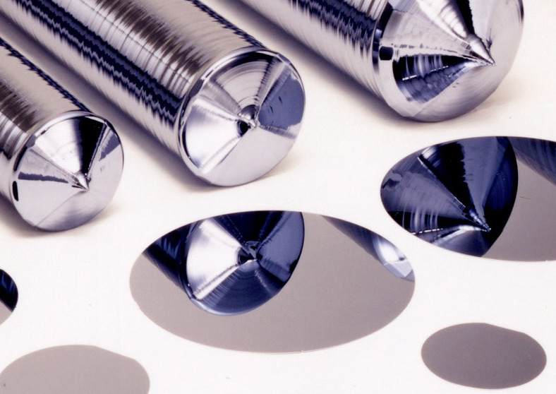
Wafers are the canvas on which transistors and then interconnects are laid in layers, and form the interstitial material that comprises the body of the chip. Because they're the foundational layer, and impurity as previously mentioned has a tendency of cascading and amplifying downstream, it's important that they're defect free. As depicted below, large ingots of silicon are created via the Czochralski process - near perfect Silicon monocrystals are slowly and carefully "pulled" from an initial seed crystal out of crucible of molten polysilicon.
This large ingot is then trimmed and sliced into the recognizable wafer. There are a number of inspection, planing, and general defect detection/removal steps in this process. The output is the perfect polished disks that form the base of modern semiconductors.
It's important to note that, outside of the Silicon, the elements in this category are primarily used in specialty chips with unique constraints (e.g. Germanium wafers are primarily used for photonics and aerospace chips) but not for modern GPUs, so for my purposes I'm not particularly interested in them.
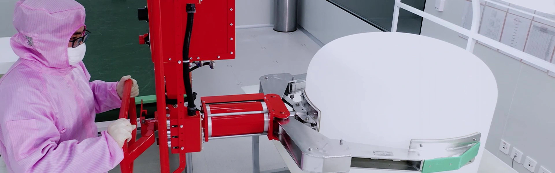
When growing huge silicon crystals, you need molten polysilicon and something to contain it. The challenge is that molten silicon has a tendency to react and form compounds with the crucible material it's contained within. This is obviously a problem if you need to grow an extremely pure silicon crystal for wafer production. To circumvent this, crucibles are made from even more pure silicon (quartz - SiO2 in this case). This ultra-pure silicon comes exclusively from Spruce Pine, NC.
Polysilicon Producers
Wacker Chemie AG
- Exec Summary: High purity precursor manufacturer
- Scale: Public, 16,972 employees, $6.5 2024 rev, $3.5bn MCAP
- Notes: Are now the largest polysilicon manufacturer in the world. Still a minority of their business. Solar quality polysilicon and silicones are their largest products, but their leading edge semiconductor quality polysilicon business is growing.
- Location: German, with substantial foreign footprint. Primary polysilicon plant is in Charleston Tennessee
- Tags: inputs, polysilicon, de
Hemlock Semiconductor
- Exec Summary: US based Corning & Shin-Etsu JV polysilicon producer
- Scale: Private, 1,350 employees, $500m 2024 rev, $1.2bn MCAP
- Notes: The vast majority of Hemlock's revenue comes from semiconductor grade polysilicon. JV is Corning (80%) & Shin-Etsu (19.5%).
- Location: Hemlock, Michigan, USA
- Tag: inputs, polysilicon, domestic, corning, shin-etsu, us
OCI Company Ltd.
- Exec Summary: Special/high value chemicals company with polysilicon arm.
- Scale: Public, 1,600 employees, $900m rev, $2.57bn MCAP
- Notes: Semiconductor polysilicon accounts for about ~25% of their revenue
- Location: Headquartered in Seoul, SK-domestic production, a number of overseas facilities and partnerships in China & US.
- Tags: inputs, polysilicon, sk
Wafer Manufacturers
Shin-Etsu Chemical (SEH)
- Exec Summary: Photoresist & wafer producer
- Scale: public, 26k employees, $16bn rev, $63bn mcap
- Notes: #1 producer of 300mm wafers (30% mshare), photoresists and litho consumables (~10% mshare), rare earths, CMP pads, etc. Semiconductor activity makes up the bulk of their revenue, with leading node activity accounting for ~30%
- Location: HQ in Tokyo, JP, but has a global footprint
- Tags: inputs, wafers, photoresists, rees, cmp, jp
SUMCO
- Exec Summary: Silicon wafer pure play
- Scale: public, 10k employees, $2.6bn rev, $2.2bn mcap
- Notes: #2 producer of 300mm wafers (20% mshare) behind SEH, 80% of total revenue is 300mm wafers and 30-45% is specifically leading edge. Contracts are quite tight, and SUMCO (and others) are able to lock in customers for multiyear commitments
- Location: HQ in Tokyo, JP, with limited footprint elsewhere.
- Tags: inputs, wafers, silicon, jp
GlobalWafers
- Exec Summary: Silicon wafer pure play with major US footprint
- Scale: public, 7.3k employees, $1.9bn rev, $5bn mcap
- Notes: #3 wafer producer (behind Shin-Etsu & SUMCO) with 17% mshare. Has major US manufacturing presence in Sherman, TX so gives it unique geopolitical positioning. 300mm wafers account for 60% of revenue, and revenue from leading edge is about 35%.
- Location: HQ in TW, major manufacturing in Sherman, TX & St. Peters, MI, US
- Tags: inputs, wafers, silicon, tw, us
Siltronic AG
- Exec Summary: Silicon wafer pure play
- Scale: public, 4k employees, $1.5bn rev, $1.2bn mcap
- Notes: 4th largest supplier of silicon wafers, accounting for 15% of the 300mm market. new fully automated singapore facility.
- Location: HQ in Munich, Germany, manufacturing in Germany & Singapore
- Tags: inputs, wafers, de, sp
High Purity Quartz Producers
Sibelco
- Exec Summary: Mining & refining of sand and other non-metallic industrial minerals
- Scale: public, 5,020 employees, $2.5bn rev, $1.8bn mcap
- Notes: Largest supplier of High Purity Quartz (HPQ) worldwide, which they mine and refine in Spruce Pine, NC. It's unclear how much of their revenue is made up by HPQ, but likely a substantial portion
- Location: HQ Antwerp, Belgium, but operates hundreds of production sites worldwide
- Tags: inputs, silicon, hpq, be, us, mining
The Quartz Company (TQC)
- Exec Summary: High purity quartz miner & refiner
- Scale: private, 350 employees, $50m rev, $200 mcap
- Notes: JV between Imerys SA (US) & Norsk Mineral AS. Focuses exclusively on Spruce Pine HPQ, and may represent 30% of total market
- Location: HQ Oslo, Norway, processing facility in Spruce Pine, NC
- Tags: inputs, silicon, hpq, no, us, mining
Momentive (KCC Corporation subsidiary)
- Exec Summary: Specialty materials company that produces HPQ, silicon, ceramics
- Scale: private, 9,200 employees, $6.5bn rev, ?
- Notes: Large & somewhat diverse multinational founded in NY that has been acquired by korean company KCC Corporation. Is a minor player in HPQ, which may represent ~10% of their overall business
- Location: HQ in Niskayuna, NY, with over 50 sites across the americas and asia
- Tags: inputs, silicon, hpq, no, us, mining
Dopants & ion-implantation gases
One of the first steps (FEOL) in SM is the implantation of transistors into the blank silicon wafer - these transistors are formed within the base layer by replacing silicon atoms in the lattice with positive (Boron) or negative (Phosphorous) dopants in precise locations. This is done by shooting a precisely controlled ion plasma stream at the wafer - a bit like shooting a machine gun at a concrete block, where the bullets are the ions. The silicon wafers are then heated in an annealing process to heal any newly created surface defects.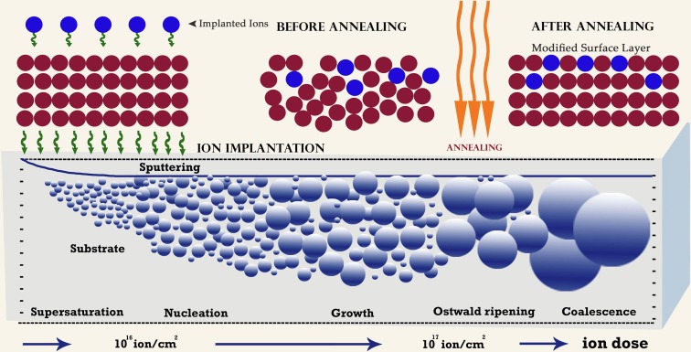
Dopant Gas Producers
Dopant gases are supplied by huge industrial chemical multinationals, for whom SM related activities represent only a small portion of their business activities.
Linde
- Exec Summary: World's largest industrial gases & engineering company.
- Scale: public, 65k employees, 33bn rev, 217bn mcap
- Notes: Semiconductor related activities accounted for only ~9% of total revenue. Primary overall market is US (32% of sales), with remaining spread throughout the world. As is the case for other industrial gas suppliers, in addition to the raw, purified gas, they supply huge amounts of additional infrastructure to store, clean, and transport the gas on the fab, as well as dedicated technicians to service the equipment.
- Location: HQ in Woking, England. Tax domicile in Ireland
- Tags: inputs, gases, uk, dopants
Air Liquide
- Exec Summary: Industrial gases for medical, chemical, and electronics manufacturers
- Scale: public, 68k employees, $30bn rev, $120bn mcap
- Notes: 2nd largest industrial gas provider behind Linde, approximately 16% overall mshare. Large producer of cleaning gases and CVD precursors. In line with Linde, about ~9% of revenue comes from semiconductor business lines.
- Location: HQ in Paris, FR major industrial sites across JP, CN, DE, US, KSA
- Tags: inputs, gases, fr, dopants, deposition
Air Products & Chemicals
- Exec Summary: Industrial gases & related equipment
- Scale: public, 23k employees, $12b rev, $60bn mcap
- Notes: 3rd largest supplier of primary gases used for semiconductor manufacturing.
- Location: HQ Trexlertown, Pennsylvania, US, with major manufacturing & distribution hubs worldwide
- Tags: inputs, gases, dopants, us, cvd, cleaning
Deposition gases
Chemical vapor deposition (CVD) is a method of depositing/applying materials with uniformity and precision to the wafer, either to form contacts (wiring between layers and transistors) or growing new layers of the silicon wafer after each layer step (epitaxial SiO2 crystal growth, referred to as EPI).
CVD Gas Producers
SK Materials Co.
- Exec Summary: Industrial gases with a focus on cleaning, deposition, etching, precursors, and wet chemicals.
- Scale: public, 700 employees, $3.5bn rev, $2.7bn mcap
- Notes: Very dominant in NF3 (cleaning gas), and among the top producers in other gases (CVD precursors). Approx. 20% of overall revenue is semiconductor related.
- Location: HQ SK, manufacturing in China, distribution throughout Asia
- Tags: inputs, sk, gases, cleaning, cn, cvd
Japan Target Lab
- Exec Summary: Custom designed high purity metals & ceramic sputtering targets for deposition
- Scale: private, ~100 employees, $45m rev, ??? mcap
- Notes: Specialist firm that only provides sputtering and other deposition related materials for niche/high end use cases (~5% mshare). Accounts for 80-90% of overall revenue.
- Location: HQ in Tokyo, JP
- Tags: inputs, sputtering, pvd, metallization, jp
Materion
- Exec Summary: High performanced engineered materials - specialty metals, inorganic chemicals, precision optics, and deposition materials.
- Scale: public, 3k employees, $1.7bn rev, $1.6 mcap
- Notes: ~20% of mshare in metalization/deposition inputs (high purity sputtering targets). SM related activites account for 12% of overall revenue. Materion acquired Heraeus' high performance target metals business for $30m in 2016
- Location: Cleveland, OH, US, but has global footprint.
- Tags: inputs, metallization, sputtering, pvd, deposition, us
Umicore
- Exec Summary: Materials technology and recycling for automotives and semiconductors
- Scale: public, 11k employees, $3.9bn rev, $2.6bn mcap
- Notes: ~15% of overall revenue is semiconductor related, and ~7% is related to leading node. Umicore makes metal deposition precursors and other nickel/metallic compounds used in interconnects & vias. They also supply high purity germanium
- Location: HQ Brussels, BE, large facilities in the US & throughout Asia
- Tags: inputs, metallization, cvd, be, germanium
Metallisation & PVD targets
Physical vapor deposition (PVD) is another method of depositing/applying materials with uniformity and precision to the wafer. This is typically done via sputtering, which can be imagined as splashing a nearby puddle of a material so as to cover an adjacent face with that material. This is done to place metallic interconnects and vias that link transistors and form circuits.
Metallisation & PVD Input Producers
Umicore
- Exec Summary: Materials technology and recycling for automotives and semiconductors
- Scale: public, 11k employees, $3.9bn rev, $2.6bn mcap
- Notes: ~15% of overall revenue is semiconductor related, and ~7% is related to leading node. Umicore makes metal deposition precursors and other nickel/metallic compounds used in interconnects & vias. They also supply high purity germanium
- Location: HQ Brussels, BE, large facilities in the US & throughout Asia
- Tags: inputs, metallization, cvd, be, germanium
Japan Target Lab
- Exec Summary: Custom designed high purity metals & ceramic sputtering targets for deposition
- Scale: private, ~100 employees, $45m rev, ??? mcap
- Notes: Specialist firm that only provides sputtering and other deposition related materials for niche/high end use cases (~5% mshare). Accounts for 80-90% of overall revenue.
- Location: HQ in Tokyo, JP
- Tags: inputs, sputtering, pvd, metallization, jp
Materion
- Exec Summary: High performanced engineered materials - specialty metals, inorganic chemicals, precision optics, and deposition materials.
- Scale: public, 3k employees, $1.7bn rev, $1.6 mcap
- Notes: ~20% of mshare in metalization/deposition inputs (high purity sputtering targets). SM related activites account for 12% of overall revenue. Materion acquired Heraeus' high performance target metals business for $30m in 2016
- Location: Cleveland, OH, US, but has global footprint.
- Tags: inputs, metallization, sputtering, pvd, deposition, us
Etch & chamber-clean gases
Etching is done to precisely remove material from the wafer (namely silicon) so as to replace it with interconnects, vias, and other components of ICs. This is done by blasting the wafer with ionized plasma gases. The important shared characteristic of these gases is their ability to eat away silicon compounds (with their free Flourine) - this is useful both in etching, e.g. carving patterns into silicon wafers, and cleaning, removing silicon compounds that form on the tool, enclosure, and in unwanted areas after process steps that add silicon.
Cleaning Gas Producers
SK Materials Co.
- Exec Summary: Industrial gases with a focus on cleaning, deposition, etching, precursors, and wet chemicals.
- Scale: public, 700 employees, $3.5bn rev, $2.7bn mcap
- Notes: Very dominant in NF3 (cleaning gas), and among the top producers in other gases (CVD precursors). Approx. 20% of overall revenue is semiconductor related.
- Location: HQ SK, manufacturing in China, distribution throughout Asia
- Tags: inputs, sk, gases, cleaning, cn, cvd
Air Liquide
- Exec Summary: Industrial gases for medical, chemical, and electronics manufacturers
- Scale: public, 68k employees, $30bn rev, $120bn mcap
- Notes: 2nd largest industrial gas provider behind Linde, approximately 16% overall mshare. Large producer of cleaning gases and CVD precursors. In line with Linde, about ~9% of revenue comes from semiconductor business lines.
- Location: HQ in Paris, FR major industrial sites across JP, CN, DE, US, KSA
- Tags: inputs, gases, fr, dopants, deposition
BASF SE
- Exec Summary: Largest chemical producer in the world, provides a number of wet chemicals for cleaning & stripping.
- Scale: public, 111k employees, $75bn rev, $44bn mcap
- Notes: Global chemicals giant that supplies a handful of lower importance chemicals used in cleaning & stripping, SM related activities likely accounts for less than 1% of their revenue
- Location: HQ in DE, global footprint
- Tags: inputs, chemicals, cleaning, stripping, de, large
Wet chemicals & cleaning agents
There are countless initial and intermediary cleaning steps. Remember, impurities compound and must be avoided. So numerous chemical baths and cleaning steps are required from the moment the wafer enters the fab right up until its departure. Some of these steps are uniform, e.g. a sacrificial layer is removed, and others are extremely precise, etching away unwanted material in certain locations.
Wet Chemical & Stripping Agent Companies
BASF SE
- Exec Summary: Largest chemical producer in the world, provides a number of wet chemicals for cleaning & stripping.
- Scale: public, 111k employees, $75bn rev, $44bn mcap
- Notes: Global chemicals giant that supplies a handful of lower importance chemicals used in cleaning & stripping, SM related activities likely accounts for less than 1% of their revenue
- Location: HQ in DE, global footprint
- Tags: inputs, chemicals, cleaning, stripping, de, large
Photoresists & lithography
We now reach the most important and complex step in SM - photolithography. While the base inputs for this step on a material side are not nearly as involved as the machinery and process around it, they are still closely coupled (new developments in the machinery require complementary developments in the material inputs). The goal of this step is to produce a very precise but temporary layer on top of the wafer that is later used to selectively shield/expose underlying wafer areas for etching. Imagine a spray paint stencil, where the areas covered by the stencil are protected from the paint but the areas exposed are covered, enabling a precise pattern from an imprecise application source. The way this stencil or mask is applied to the wafer is by first covering the wafer in a temporary photoresist polymer layer, and then shining extreme ultraviolet light on that photoresist layer through a mask/reticle, thus transferring our desired pattern into the photoresist layer. We can then develop and strip away the unexposed parts of the of the photoresist, and use the resulting physical mask to perform the etch. The inputs for this step are the photoresist polymers which are applied in a thin coat on the wafer, and some other treatment chemicals to further improve the accuracy and capabilities of the photoresist.
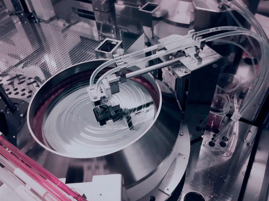
Chemical Amplified Resists (CARs) are primarily the domain of Japanese manufacturers JSR and TOK. They've taken a number of steps to solidify their monopoly in the photoresist market, like embedding full time engineers with ASML, Nikon, Canon, etc, to cooperatively fine tune compounds and provide technical knowledge transfer.
Photoresist Manufacturers
JSR (JSR Micro, Inpria)
- Exec Summary: Lithography resists, anti-reflective coatings, CMP slurries
- Scale: private, 8k employees, $2.7bn rev, $6bn mcap
- Notes: One of the 2 primary producers of photoresist polymers & anti-reflective coatings with about a 30% mshare. Provides end to end services, including qualification, R&D, and embedded engineers at ASML, Nikon, Canon, etc. Taken private in 2024 by the Japan Investment Corp. Acquired Inpria in 2021 for Metal Oxide Resist (MOR) patents, leading node production may be shifting to MOR from liquid polymers (see capillary action and other defects of liquid photoresists).
- Location: HQ Tokyo, JP & Sunnyvale, CA, production in BE, support centers throughout Asia. Inpria HQ in Corvallis, OR, US
- Tags: inputs, litho, photoresist, jp, mor
TOK
- Exec Summary: Photoresist and other litho chemicals and equipment specialist
- Scale: public, 2k employees, $1.35bn rev, $2.9bn mcap
- Notes: Leading supplier (>20% mshare) of leading node (<=7nm) photoresist chemicals. Largest pure play photoresist company.
- Location: HQ in JP, regional support offices in TW and SK
- Tags: inputs, photoresist, litho, jp
Fujifilm
- Exec Summary: Image development and associated chemicals, photoresist supplier
- Scale: public, 73k employees, $22bn rev, $26bn mcap
- Notes: Top 5 photoresist producer, focusing on a comprehensive suite of products for full imaging lifecycle. Acquired Entegris' electronic chemicals unit to expand CMP business. Has an 8% mshare in photoresist market. Electronic materials as a whole represent only about 8% of total revenue, however almost all of that revenue is related to lead edge node products.
- Location: HQ in Tokyo, JP, global footprint
- Tags: inputs, photoresist, litho, cmp, jp
Dongjin Semichem
- Exec Summary: Photoresist and lithography consumables
- Scale: public, 1.4k employees, $1bn rev, $1bn mcap
- Notes: ~90% of revenue comes from EUV and other photoresists, with Dongjin's share of the photoresist market around 5%. They are a strategically important supplier though, as they're the only SK based photoresist manufacturer, so SK consumers like Samsung and SK Hynix rely on them to hedge geopolitical risk.
- Location: HQ in Seoul, SK, with manufacturing throughout SK and in China
- Tags: inputs, photoresist, sk, litho
CMP consumables
Chemical Mechanical Planarization (CMP) is another removal step, a high precision physical layer removal to flatten a wafer and uniformly remove materials. Think of it like sanding a layer off the wafer. Doing this (with precision) requires very specific abrasives called CMP slurries.
CMP Consumable Manufacturers
Dow Inc.
- Exec Summary: Large industrial hydrocarbon processor, produces plastics and specialty silicones
- Scale: public, 36k employees, $43bn rev, $20bn mcap
- Notes: Huge petrochemical processor, small arm that produces solvents, cmp, & litho chemicals. SM related activities account for less than 1% of total revenue.
- Location: HQ Midland, MI, US, but global footprint
- Tags: inputs, cmp, litho, solvents, us
Fujifilm
- Exec Summary: Image development and associated chemicals, photoresist supplier
- Scale: public, 73k employees, $22bn rev, $26bn mcap
- Notes: Top 5 photoresist producer, focusing on a comprehensive suite of products for full imaging lifecycle. Acquired Entegris' electronic chemicals unit to expand CMP business. Has an 8% mshare in photoresist market. Electronic materials as a whole represent only about 8% of total revenue, however almost all of that revenue is related to lead edge node products.
- Location: HQ in Tokyo, JP, global footprint
- Tags: inputs, photoresist, litho, cmp, jp
An Aside: Rare Earth Elements
Rare Earth Elements (REEs) are often held up as examples of supreme Chinese dominance. It's true that China is the largest producer of REEs. But that's not the whole story.
First, it's important to understand the how REEs are used in modern semi manufacturing. There are two relevant fundamental applications for which REEs are particularly useful: in improving the strength and lifespan of permanent magnets, and in producing high power lasers. In the direct production of GPU clusters like an H100, only small amounts of Neodymium and Dysprosium are used to in the construction of compact and powerful fans. In essence, REEs are not a particularly essential input for individual semiconductors or finalized clusters. Instead, they are most important in the production of the machines on the fab line - ASML's EUV machines require much larger quantities of various REEs (both for ultra high powered lasers and for precision electromagnets). This is also true for a litany of other cleaning, inspection, and deposition machines. And in the context of global demand for REEs, the semiconductor manufacturers and their machine suppliers like ASML represent only a very small fraction (<5%). The primary market for REEs is in EVs, photovoltaics, and wind turbines.
Second, it should be understood how REEs are extracted and refined. REEs can be found almost everywhere - the challenge is cost effective and environmentally sensitive extraction and processing. Namely, the extraction process is (in its current cost competitive form) extremely toxic - acidic solvents are necessary to properly isolate REEs at sufficient purity levels, and these acidic solvents eventually become radioactive wastewater that must be stored in huge volumes. America and Europe were once dominant despite these hurdles. But China, with heavily subsidized mining and very little consideration for environmental externalities of these dirty processes was able to price western competitors out of the market completely. Western countries also (probably correctly) concluded that the environmental costs were not worth subsidizing at the time, and so were happy to outsource REE processing.
REE processing is not extremely complex - it's just toxic. And it can be done more cleanly, just not in a price competitive manner (in the current regime). It will take time and capital to onshore or nearshore REE production, but it simply is not a long term bottleneck.